Destacando el papel de IMB-CNM en el 37º Simposio Internacional del IEEE sobre Circuitos Integrados y Dispositivos Semiconductores de Potencia
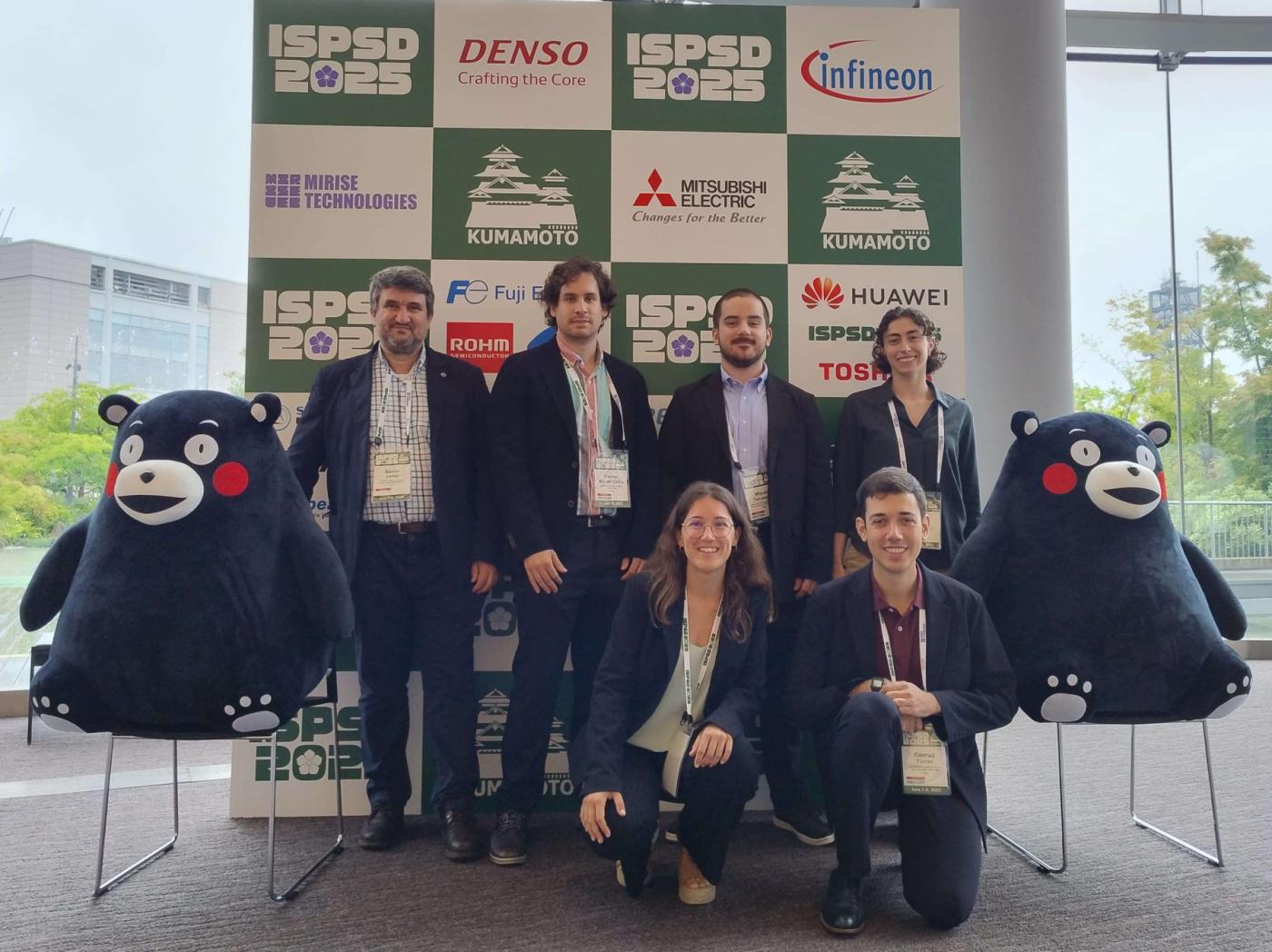
Por primera vez, personal investigador del grupo de Dispositivos y Sistemas de Potencia del IMB-CNM ha presentado cinco contribuciones en el 37º Simposio Internacional del IEEE sobre Circuitos Integrados y Dispositivos Semiconductores de Potencia (ISPSD), la principal conferencia internacional sobre dispositivos semiconductores de potencia, celebrada el pasado mes de junio en Japón
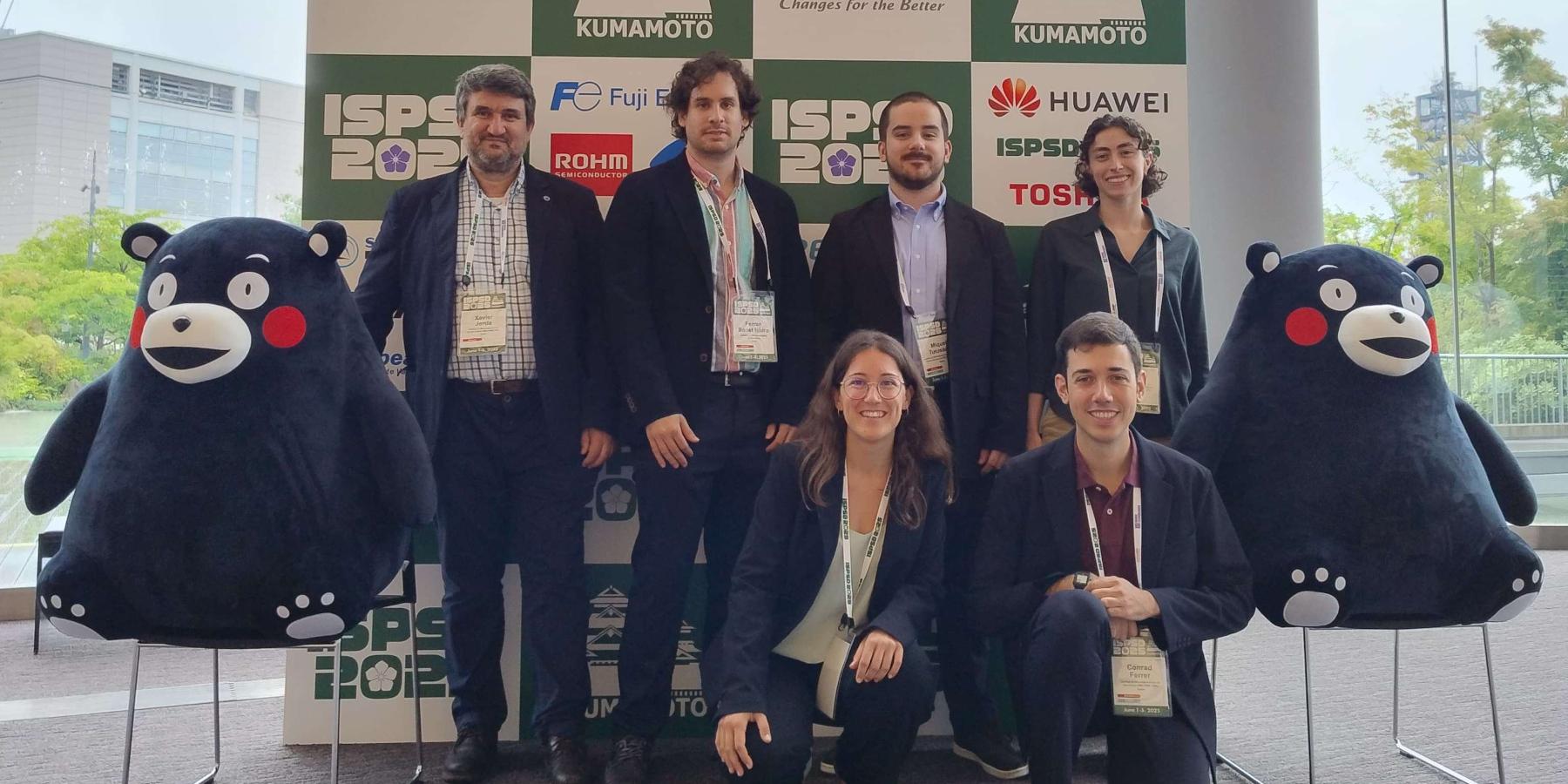
Por primera vez, personal investigador del Grupo de Dispositivos y Sistemas de Potencia (PDS) del IMB-CNM presentó cinco contribuciones en la principal conferencia internacional sobre dispositivos semiconductores de potencia, el 37º Simposio Internacional IEEE sobre Circuitos Integrados y Dispositivos Semiconductores de Potencia (IEEE International Symposium on Integrated Circuits and Power Semiconductor Devices, ISPSD). El evento se celebró del 1 al 5 de junio en Kumamoto (Japón) y reunió a los principales protagonistas mundiales en este campo, tanto industriales como académicos.
La ISPSD es una conferencia internacional de primer orden para la presentación y el debate de todos los aspectos de las tecnologías de dispositivos semiconductores de potencia y circuitos integrados de potencia. Los semiconductores de potencia son una de las tecnologías facilitadoras clave para el despliegue de soluciones de energías renovables, redes inteligentes para la distribución segura y eficiente de la energía eléctrica y la electrificación de los procesos industriales como herramienta para alcanzar los objetivos de transición energética de nuestra sociedad.
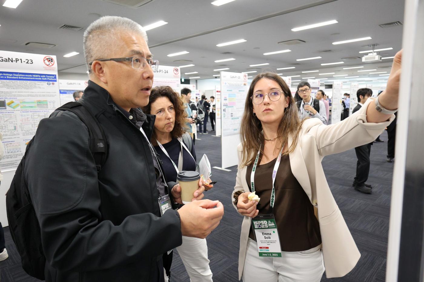
Este año, cinco investigadores predoctorales del grupo PDS presentaron sus contribuciones. Mariana Raya hizo una presentación oral, mientras que Emma Solà, Ferran Bonet, Conrad Ferrer y Miquel Tutusaus participaron en la sesión de pósteres. Todas las presentaciones abordaron algunos de los problemas más acuciantes que afectan a la integración y caracterización avanzada de dispositivos semiconductores de potencia, generando un gran interés y suscitando debates científicos con otros participantes. Además, Xavier Jordà, investigador del IMB-CNM, fue miembro del Comité Técnico del Programa y presidió la sesión sobre Tecnologías de encapsulado durante la conferencia.
A continuación, se ofrece un resumen del contenido de las cinco contribuciones presentadas en la ISPSD.
SiC MOSFET Chip Embedded Switching-Cell for Multilevel Converters
Presentado por Mariana Raya.
El chip embedding se perfila como una prometedora tecnología avanzada de encapsulado que ofrece importantes ventajas sobre los métodos convencionales en cuanto a rendimiento, fiabilidad y miniaturización. Este método de integración permite combinar de forma sencilla y rentable componentes SMD estándar sobre PCB (placas de circuito impreso) y dispositivos de potencia integrados en la propia placa. Esta característica se consideró de gran interés para el desarrollo de módulos de alimentación inteligentes que integren celdas de conmutación modulares y escalables en el marco del proyecto SCAPE de Horizon Europe.
Mariana Raya explicó el diseño, desarrollo y caracterización de una celda de conmutación inteligente para convertidores multinivel, utilizando tecnología de incrustación de chip y MOSFETs de potencia de carburo de silicio (SiC) de 750V y 12mΩ. El diseño de la celda de conmutación se optimizó en términos de inductancia parcial y resistencia térmica mínimas. Los resultados de la simulación coinciden con los datos experimentales, mostrando una resistencia térmica de la unión a la cara posterior de 0,63 K/W y una inductancia parásita de 2,7nH a 10MHz. El rendimiento eléctrico y la funcionalidad de la celda también se validaron experimentalmente hasta 400 V, 30 A y una frecuencia de conmutación de 100 kHz, lo que confirma el interés de la incrustación del chip para la integración de módulos de potencia inteligentes en la gama media de tensión/potencia.
Chip-level Interconnection Techniques for Chip Embedding Integration of SiC MOSFETs
Presentado por Emma Solà.
El fundamento del enfoque chip-embedding consiste en introducir los dispositivos semiconductores de potencia dentro de las placas de circuito impreso de un determinado circuito convertidor, consiguiendo altos niveles de integración. El trabajo presentado por Emma Solà se centró en las técnicas de interconexión die-level superior e inferior necesarias para habilitar los contactos eléctricos de los dispositivos embebidos. Se presentó una novedosa técnica propia para remetalizar selectivamente con cobre las almohadillas de contacto de cualquier dispositivo mediante enmascaramiento de sombra dura, para permitir posteriores contactos de microvía estándar durante el proceso de fabricación de la placa de circuito impreso. En este trabajo se utilizó la técnica para remetalizar los pads de puerta y fuente de MOSFET de SiC de 750V-12mΩ, que luego se unieron a marcos de plomo de Cu con una capa robusta de micro/nano partículas de plata sinterizadas. Estos conjuntos se integraron con éxito para implementar celdas de conmutación elementales utilizadas en convertidores de potencia multinivel diseñados para aplicaciones de tracción eléctrica en el marco del proyecto SCAPE.
Measurement of Free-Carrier Density in a 1.2 kV SiC Schottky Diode under Overstress Conditions
Presentado por Ferran Bonet.
El desarrollo de nuevos dispositivos de potencia basados en materiales novedosos y estructuras innovadoras requiere técnicas avanzadas de caracterización electrotérmica a nivel de matriz (die-level). Entre estas técnicas, el método de deflexión interna de infrarrojos y láser (IIR-LD) destaca como una potente herramienta para medir variables térmicas y eléctricas en el interior de los dispositivos durante su funcionamiento. Ferran Bonet fue el primero en demostrar la aplicación con éxito del método IIR-LD para medir el perfil de densidad de portadores en un diodo Schottky de SiC de 1,2 kV en condiciones de sobrecorriente. Este tipo de sobrecarga eléctrica induce un alto nivel de inyección en la región de deriva en la extensión de la terminación de la unión, activando de forma efectiva el comportamiento del diodo PiN.
Para ello, Bonet abordó retos clave en el postprocesado de datos IIR-LD: desacoplar los efectos de la temperatura de la densidad de portadores en las señales de deflexión y deconvolver para el diámetro relativamente grande del rayo láser (~16 μm) de la concentración de portadores medida. Los resultados experimentales en la región de deriva muestran una excelente concordancia con las simulaciones, revelando densidades de portadores que oscilan entre 2,73×10¹⁶ y 3,47×1016 cm-³. Además, las mediciones en la región del sustrato indican una ionización del dopante impulsada por la temperatura. Todos estos resultados serán muy relevantes para el desarrollo de dispositivos de SiC de nueva generación en el proyecto SAFEPOWER de Horizon Europe.
Thermal Analysis of Current Crowding in IGBTs under Stressful Operation in Resonant Converters
Presentado por Conrad Ferrer.
La monitorización de la temperatura en semiconductores de potencia es un área de investigación clave debido a su impacto en la fiabilidad del sistema. Los métodos de medición con resolución espacial proporcionan distribuciones térmicas superficiales que permiten detectar puntos calientes inducidos, por ejemplo, por fenómenos de aglomeración de corrientes. Conrad Ferrer presentó por primera vez la tensión eléctrica a nivel de matriz debida a condiciones de aglomeración de corrientes analizadas mediante termografía infrarroja (IR) en un transistor IGBT que funciona en un convertidor resonante de medio puente fuera del régimen de conmutación de tensión cero (ZVS) de 150 a 75 kHz de frecuencia de conmutación. El procesamiento personalizado de imágenes IR con coeficientes de Fourier y reconstrucción temporal permitió la monitorización no invasiva en 10 µm submilisegundos del mapa térmico del dispositivo durante la operación de conmutación, identificando áreas sobrecalentadas en regiones de baja impedancia en una escala temporal de decenas de microsegundos.
Non-Intrusive Online Junction Temperature Monitoring in Si and SiC Power MOSFETs
Presentado por Miquel Tutusaus.
Con el aumento de los sistemas electrónicos de potencia debido a la descarbonización de la industria, es importante asegurar un funcionamiento fiable en diferentes condiciones de estrés. En este sentido, la temperatura de unión de los dispositivos semiconductores de potencia es un parámetro clave a tener en cuenta a la hora de diseñar y operar sistemas de potencia para asegurar una fiabilidad adecuada. Sin embargo, la medición en línea de la temperatura de unión de los dispositivos de potencia en condiciones de conmutación de alto voltaje es una tarea muy difícil. Miquel Tutusaus presentó un método no intrusivo basado en un circuito de sujeción rápida y una tabla de consulta para utilizar la caída de tensión en estado ON de los dispositivos de potencia como parámetro eléctrico sensible a la temperatura (TSEP). Este método permite monitorizar la temperatura de unión de los MOSFET de Si y SiC durante el funcionamiento del convertidor, consiguiendo desviaciones de medición de la temperatura en estado estacionario inferiores a 1 °C. La solución propuesta será de principal interés para convertidores industriales como las cocinas de calentamiento por inducción desarrolladas por la empresa BSH.