i-ELPHOS: Integrated Electrophotonic Sensor
The i-ELPHOS project has received funding from the European Union's Horizon 2020 research and innovation programme under Marie Skłodowska-Curie grant agreement No. 801342 (Tecniospring INDUSTRY) and the Government of Catalonia's Agency for Business Competitiveness (ACCIÓ).
The research is made in collaboration with the company Sens Solutions acting as secondment entity, and led by the Photonics section of the Chemical Transducer Group (GTQ) at IMB-CNM.
Sens Solutions is a reference in the water control sector, commercializing a biofilm sensor and a portable devices for rapid analysis. GTQ is an interdisciplinary research group at the National Microelectronics Center (IMB-CNM), the largest microelectronics research and development center in Spain, which belongs to the Spanish National Research Council (CSIC), the largest public institution in Spain dedicated to research and one of the most renowned of the European Research Area (ERA). GTQ is part of TECNIO, a quality mark awarded by ACCIÓ that includes the research agents with the most technology transfer potential.
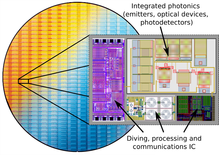
The goal of i-ELPHOS is to develop a true fully integrated electrophotonic sensor platform applied to the detection of biofouling/films in water. The concept is based in the monolithic integration of light emitters, planar waveguides, photodetectors, and driving and processing electronics. This is done using standard silicon wafers as substrate as well as materials and fabrication facilities available in the IMB-CNM, which are standard for microelectronics industry, enabling wafer-scale fabless development, mass production, high yields, and low costs.
Figure 1 presents the concept of a monolithic chip integrating electronics and photonics in wafer-scale fabrication.
The system is built around a light emitting source based on a nano-structured silicon material obtainable by standard techniques, enabling a monolithic electrophotonic emitter-waveguide-detector (EWD) architecture in which the light source is directly embedded and auto-aligned with the waveguide. This philosophy allows for true cost-effective lab-on-a-chip (LOC) beyond the state of the art due to two main advantages: 1. No external optical elements and light sources thanks to the unique light emitter; 2. True availability of all the stages of the operation of a sensor in a single chip, including transduction and signal processing, since it is possible to integrate the electronics in the same substrate.