Técnicas y equipos del Área de Nanolitografía
El Área de Nanolitografía se dedica a la definición de características a nivel de resolución submicrométrica, y a la caracterización de materiales, procesos y dispositivos fabricados en el instituto a escala nanométrica.
Técnicas
- Electron beam lithography (EBL)
- AFM based nanofabrication
- Nanoimprint lithography
- Focused Ion Beam (FIB)
- Scanning Electron Microscopy (SEM)
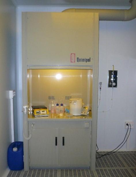
- Resist Processing
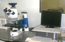
- Optical Microcope (OM)
Equipos
AFM microscope
Bruker Icon AFM
- Close-loop scanner
- Sample size up to a 150 mm wafer
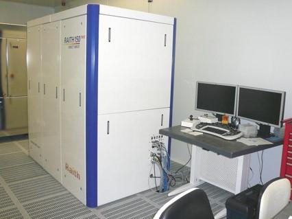
Electron beam lithography
RAITH 150 (TWO) dedicated electron beam lithography system
- From samples up to 150 mm wafers
- 0,1 to 30kV acceleration voltage
- Height Sensor
- Interferometric Stage
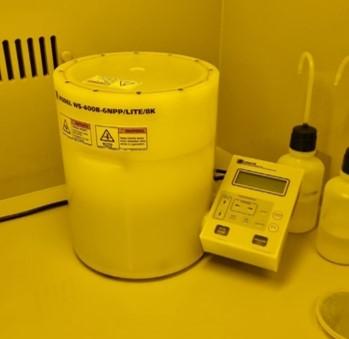
Nanoimprint lithography (NIL)
Obducat thermal nanoimprint system
- Sample size up to 150 mm wafers
- Maximum pressure: 80 bars and temperature up to 350 ºC
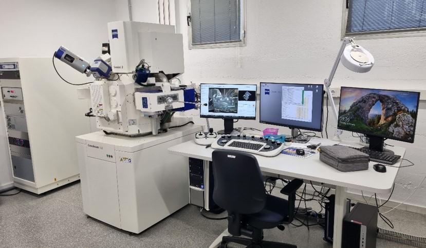
Focused Ion Beam
Zeiss Crossbeam 550L
- Sample size up to a 150 mm wafer
- Circuit editing capability
- Nanomachining capabilities
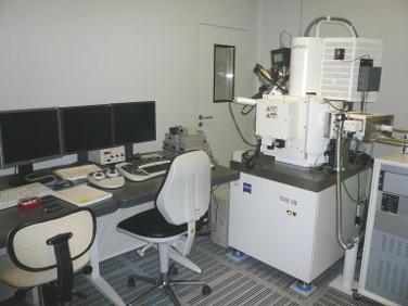
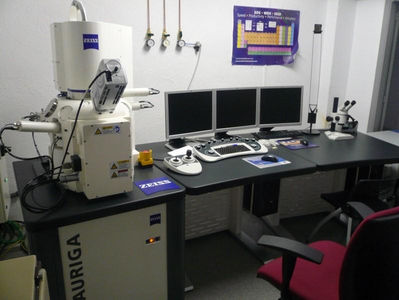
Scanning Electron Microscopy
Zeiss 1560 and Zeiss AURIGA 40 Field Emission SEMs
- 4” full acces (6 and 8 inch possible)
- EDS Oxford Detector
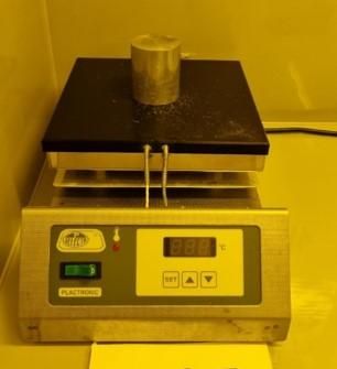
Resist Processing
Fume Hood with Laurell Spinner and Hot-Plate
- Small pieces to 6” wafers
- Hot-Plate up to 200ºC
Optical Microscopy
Zeiss AxioM1
- Manual Plate
- Bright Field and Dark Field
Capacidades disponibles
EBL nanolithography
- Lithography on positive and negative resists
- Resolution below 20 nm
- Up to 6 inch wafers in stich fields, stitch resolution below 20nm
- Mix & Match with Optical Lithography
Nanoimprint lithography
- Imprinting of polymer resists on different surfaces.
- Imprinting of polymers foils (hot-embossing)
- Resolution below 100 nm
- Imprinting area up to 4"
- "In house" technology for mould fabrication and conditioning
Focused Ion Beam (FIB)
- Nanofabrication (Ga ions): Resolution below 20 nm depending on the material.
- Gas Injection System (GIS): Pt, C, W, TEOS deposition & O2, F etching
- Omniprobe for lamella preparation.
- SmartFIB patterning software
Caracterización
Topographical characterization by AFM
- Maximum sample size: 6'' wafer
- Maximum range of images: 30 μm (X) x 30 μm (Y) x 4 μm (Z)
- Lateral resolution (depending on surface features): 1 nm
- Vertical resolution: 0.1 nm AFM
- Other SPM techniques available on request
SEM characterization
- SEM characterisation of whole wafers up to 6''
- In-Lens, SE, EBS, STEM and BSE detectors
- Oxford EDS detectors
- Metrology (automatic large area imaging) and measuring
FIB characterization
- FIB cross-sectioning
- TEM lamela preparation
- Circuit Editing.
- SEM & FIB 3DMapping (topographic and/or EDS)
Optical MicroscopyLocal electrical characterization
- Camera and computer attached
- Multiple Objectives (x5,x10,x20,x50,x100 plus condensers)
- Bright Field and Dark Field
Descarga las técnicas y capacidades del Área de Nanolitografía
Mira el Área de Nanolitografía
Personal del Área de Nanolitografía
- Xavier Borrisé (ext. 435564)
- Llibertad Solé (ext. 435557)
- Albert Guerrero (ext. 435562)