


Articles científics destacats
Aquesta secció inclou una llista dels treballs científics més destacats de l'IMB-CNM publicats en revistes incloses al Science Citation Index (SCI), per any de publicació.
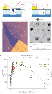
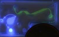
The presence of lattice defects in graphene might degrade its mechanical properties. We report a study on the elastic modulus and strength with a controlled density of defects. Counter-intuitively, the in-plane Young’s modulus increases with defect density up to 2x the initial value for a vacancy content of ~0.2%.
Nature Physics 11, 26–31 (2015)
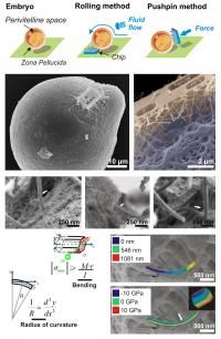
The adhesion of small silicon chips to cells has many potential applications as direct interconnection of the cells to the external world can be accomplished. Although some typical applications of silicon nanowires integrated into microsystems are focused on achieving a cell-on-a-chip strategy, we are interested in obtaining chip-on-a-cell systems. This paper reports the design, technological development and characterization of polysilicon barcodes featuring silicon nanowires as nanoscale attachment to identify and track living mouse embryos during their in vitro development.
Lab on a Chip, 15, 1508-1514 (2015)
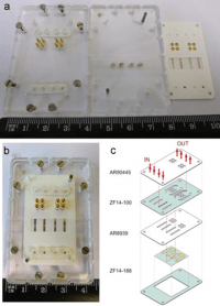
We report on the production of a low cost microfluidic device for the multiplexed electrochemical detection of magneto bioassays. As a proof of concept, the device has been used to detect Myeloperoxidase (MPO), a cardiovascular biomarker. A dual MPO mass and activity assay has been finally applied to the study of 10 real plasma samples, allowing patient classification according to the risk of suffering a cardiovascular event.
Biosensors and Bioelectronics 69, 328–336 (2015)
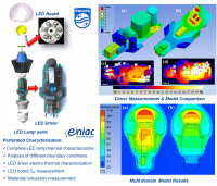
This work reports on the thermal influence of an LED (Light Emitting Diode) driver on a retrofit LED lamp, also reporting on a procedure for its thermal characterization and multi-scale modeling to optimise its integration. This study has been carried out within the Consumerizing Solid State Lighting project led by Philips and funded by ENIAC Joint Undertaking platform.
IEEE TRANSACTIONS ON POWER ELECTRONICS, VOL. 30, NO. 7, JULY 2015
A photonic lab on a chip (PhLOC), comprising a solid-state light emitter (SSLE) aligned with a biofunctionalized optofluidic multiple internal reflection (MIR) system, is presented. The SSLE is obtained by filling a microfluidic structure with a phenyltrimethoxysilane (PhTMOS) aqueous sol solution containing a fluorophore organic dye. Its performance is assessed by measuring quinolone yellow, obtaining a limit of detection (LOD) of (0.60±0.01) µM. Finally, the MIR is selectively biofunctionalized with horseradish peroxidase (HRP) for the detection of hydrogen peroxide (H2O2) target analyte, obtaining a LOD of (0.7±0.1) µM for H2O2.
Light: Science & Applications (2015) 4, e271; DOI:10.1038/lsa.2015.44
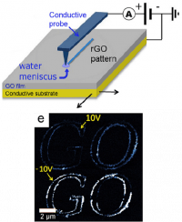
In this paper, we report on a method to reduce thin films of graphene oxide (GO) to a spatial resolution better than 100 nm over several tens of micrometers by means of an electrochemical scanning probe based lithography.
Nanotechnology 26 (2015) 285301.
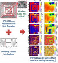
The functionality and consumption of an RFID IC supplied by Inductive Power Transfer (IPT) has been non-invasively analyzed by IR thermography.The main aspects addressed in thiswork have been: the suitability study of the proposed modulation strategies, the characterization of the coupling between coils and its effects on the RFID blocks, the RFID IC functional analysis, and the dependence of the local energy consumption on the total power delivered to the die.
IEEE Transactions on Industrial Electronics
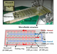
In this work an automated and reusable electrical readout system for low-cost glass slide microarrays is described. The system, which enabled the simultaneous conductimetric detection of up to 36 biorecognition events, comprises an array of interdigitated electrode transducers and a polydimethylsiloxane microfluidic structure, aligned over it.
The impedimetric system shows similar sensitivity to that of fluorescence scanners.
Biosensors and Bioelectronics 74 (2015) 698–704.
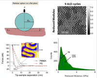
The mechanical properties of several types of block copolymer thin films have been investigated using PeakForce quantitative nanomechanical mapping. The samples consisted of polystyrene/poly(methylmethacrylate) with thickness below 50 nm and features of less than 22 nm.
Langmuir, 31 (2015) 11630
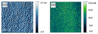
The nanomechanical properties of solvent-cast polymer thin films have been investigated using PeakForce™ Quantitative Nanomechanical Mapping. The samples consisted of films of polystyrene and poly(methyl methacrylate). Additionally, we have probed the mechanical properties of poly(styrene-b-methyl methacrylate) block copolymers (BCP) as randomly oriented thin films.
J. Micro/Nanolith. MEMS MOEMS 14 (2015) 033509.