La revolució silenciosa exhibition
La revolució silenciosa exhibition traces the 75-year history of the transistor, to which digital society owes its raison d'être. This electronic device functions as a switch that lets current pass through and is integrated into the chips that make up cell phones, hearing aids and electronic devices everywhere. Here you can read the summary of the exhibition in English, Catalan or Spanish.
The exhibition is itinerant and it has been scheduled in the following places and dates:
- Reial Acadèmia de Ciències i Arts de Barcelona (RACAB, Barcelona), from May 13th to June 21st 2024.
- Institut d'Estudis Catalans (IEC, Barcelona), from February 1st to March 7th, 2024.
- Centre Cultural Can Rajoler (Parets del Vallès), from January 10th to 30th, 2024.
- Lleialtat Santsenca (Barcelona), from November 2nd to 25th, 2023.
- FAB Casa del Mig (Barcelona), from June 5th to 28th, 2023.
- Escola Tècnica Superior d'Enginyeria de Telecomunicacions de Barcelona UPC (ETSETB-UPC, Barcelona), from April 20th to May 19th, 2023.
- Escola Tècnica Superior d'Enginyeria Industrial de Barcelona UPC (ETSEIB-UPC, Barcelona), from March 2nd to March 30th, 2023.
- UAB Science and Technology Library, from November 28, 2022 to January 12, 2023.
It is free of charge and lent for periods of at least one month. Should you wish to schedule it in your space, please contact cultura@imb-cnm.csic.es.
Many consider the transistor to be the greatest invention of the 20th century
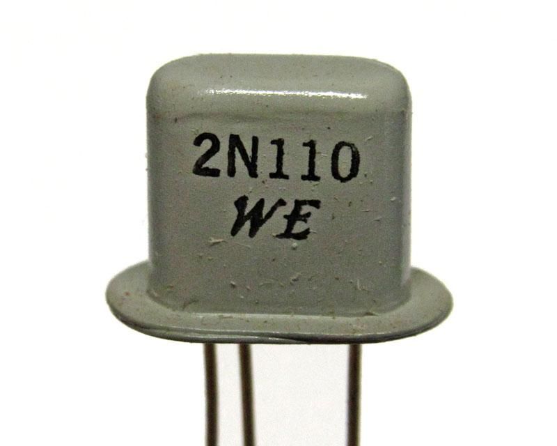
The technological revolution of the last decades has a silent and unknown protagonist: the transistor. Many experts consider it to be the most important invention of the 20th century, essential for understanding the development of microelectronics, miniaturization and the digitalization processes of our society. The transistor is a three-terminal semiconductor electronic device used to deliver an amplified output signal in response to an input signal. Have you ever wondered how many electronic devices you use every day? And how many transistors? The adventure begins in 1947...
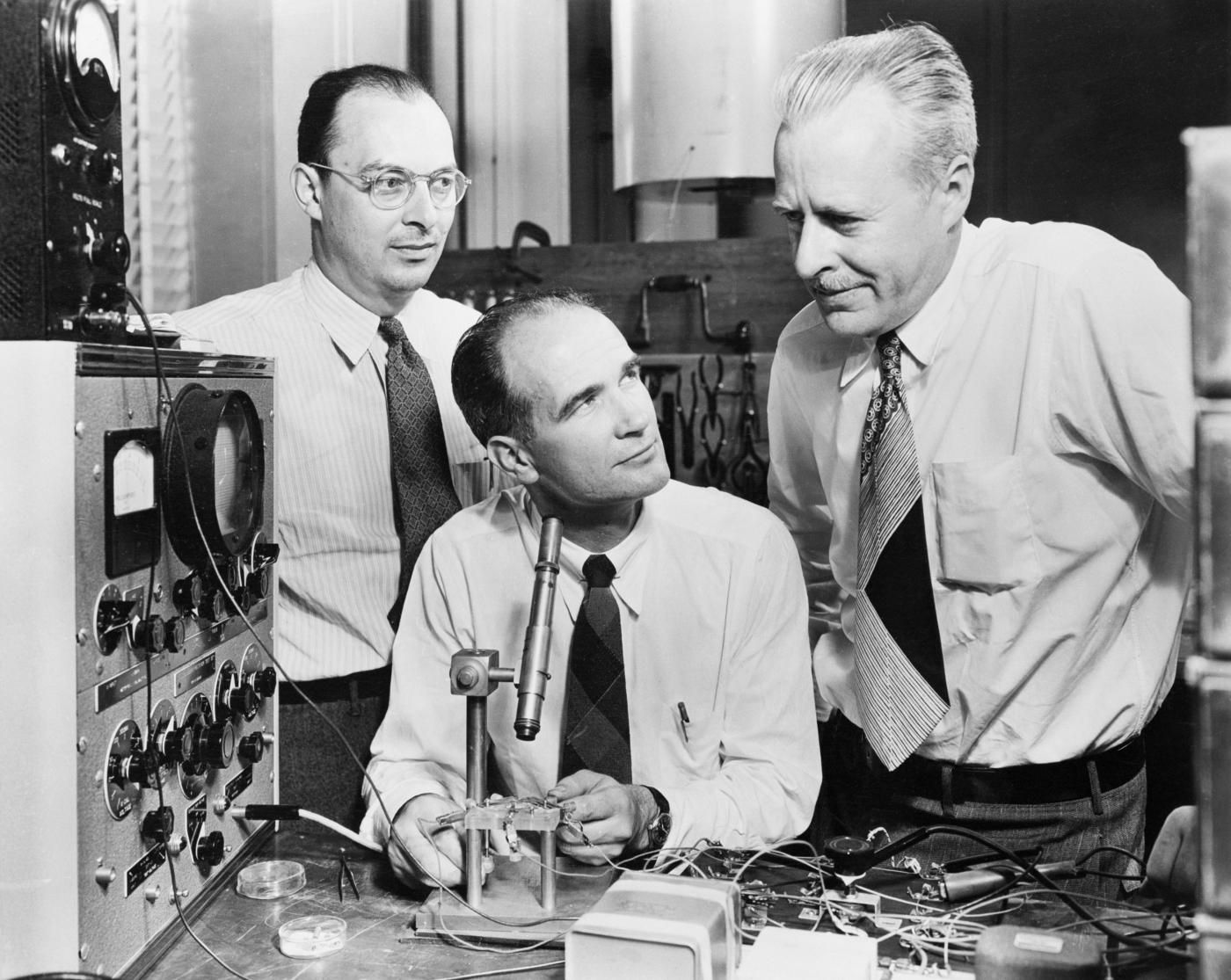
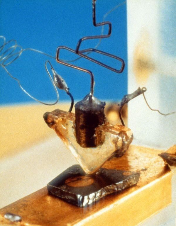
In 1947, the amplifying effect of a germanium semiconductor device, the point-contact transistor, was demonstrated
The rapid development of microelectronics began after World War II. AT&T had a research group headed by William Shockley at the Bell Labs facility in Murray Hill, USA. On December 16, 1947, physicists John Bardeen and Walter H. Brattain succeeded for the first time in demonstrating the amplifying effect of a germanium semiconductor device, the point-contact transistor. Months later, Shockley devised a much improved type of transistor: the junction bipolar transistor. All three won the Nobel Prize in Physics in 1956 for this work.

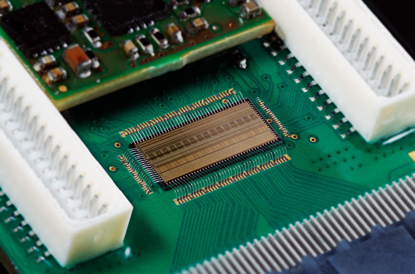
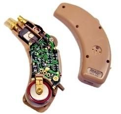
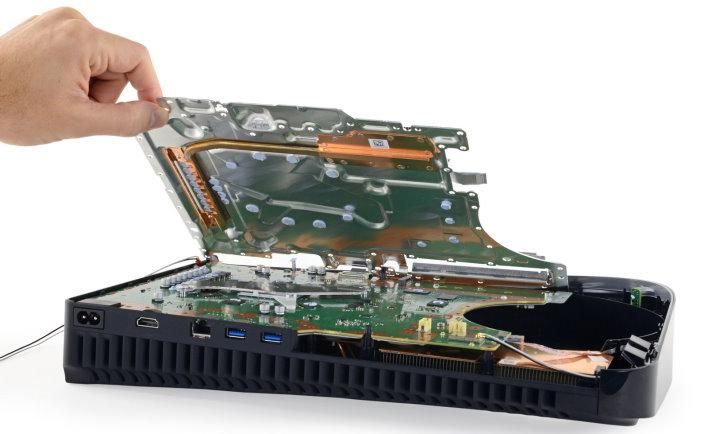
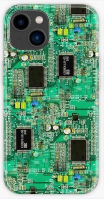
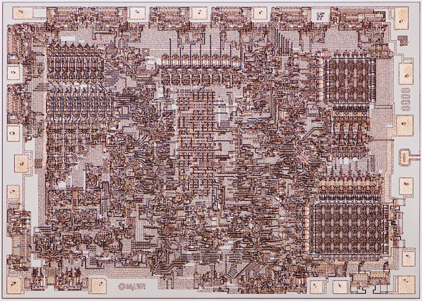
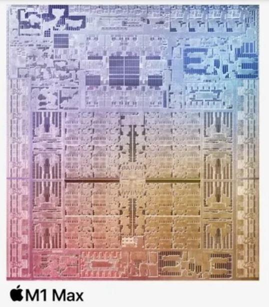
Chips or integrated circuits are small pieces of silicon that integrate millions of interconnected transistors
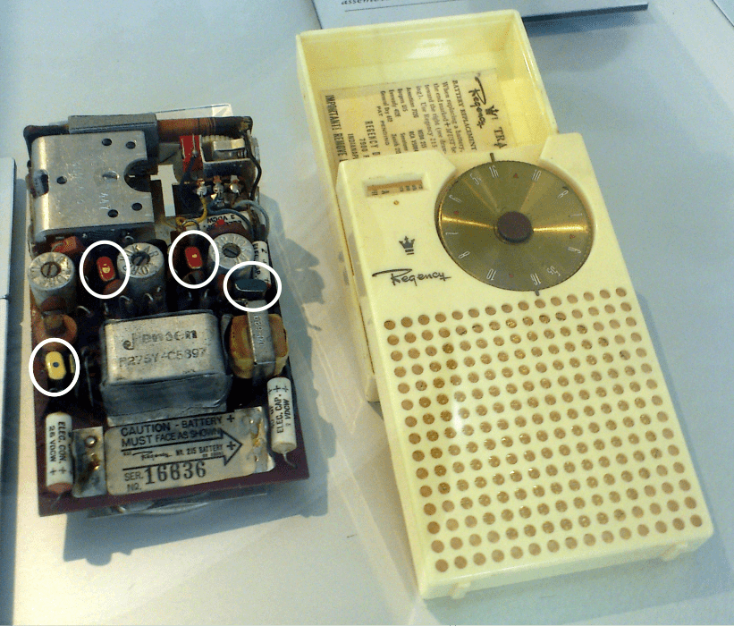
Although initially conceived as an analog amplifier device, its use as a switch, blocking or allowing the electric current to circulate, made it possible to physically specify the '1' and '0' of binary logic. Today, the microprocessor chips and memories found in the vast majority of the equipment we use every day, integrate millions of these devices interconnected with each other in small rectangular pieces of silicon that we call integrated circuits or chips.
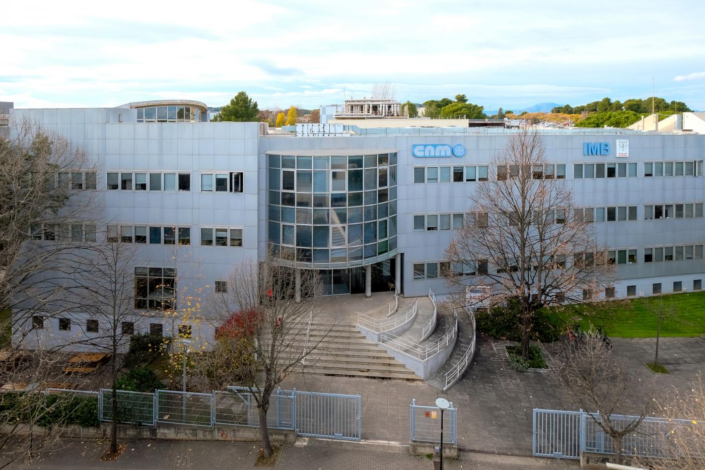
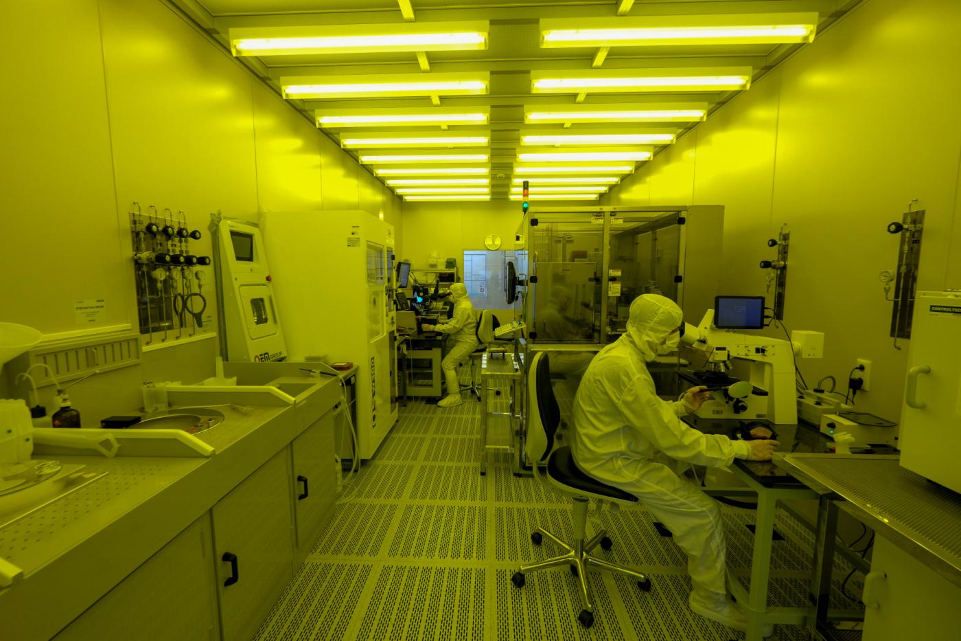
The IMB-CNM houses the Micro and Nanofabrication Clean Room, unique in southern Europe, where silicon chips can be manufactured!
The adventure of the Institute of Microelectronics of Barcelona (IMB), created in 1985 and headquarters of the National Microelectronics Center (CNM), is linked to the discovery of the transistor. It is located in Cerdanyola del Vallès and has a 1,500 m² Clean Room (with the category of Unique Scientific and Technical Infrastructure, ICTS) where silicon chips can be manufactured, which has allowed the development of research lines in micro- and nanotechnologies. We hope to participate many more years in this adventure that still has many things to say!