The CSIC INVESTIGA magazine collects the IMB-CNM's research in energy on storage and electrification
Issue 3 of the CSIC INVESTIGA magazine, coordinated by the CSIC Communications team, focuses on Energy and the current challenges presented by its research: renewable energy generation, industry conversion, storage and transformation

The latest issue of the CSIC INVESTIGA magazine focuses on Energy and collects research from the organization's groups and institutes devoted to its study. The IMB-CNM is mentioned on several occasions for its work on self-powered low-consumption sensors, for the research for materials that replace silicon or for the investigation into the reliability of electronic components. The Clean Room, a large facility where semiconductors for energy applications can be manufactured, also stands out.
CSIC INVESTIGA is a publication coordinated by the CSIC Communications team and is published twice a year. Each issue deals with one of the great challenges of today's society and collects the efforts of the CSIC centers and units in the matter.
Towards clean, safe and efficient energy
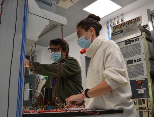
The article that opens the issue summarizes the great challenges facing society in the field of energy and the CSIC's research in the field. Xavier Jordà, researcher in the Power Devices and Systems group and deputy director of the institute, talksakes stock about the efforts in industrial electrification to achieve industrial decarbonization in 2050.
Abundant metals challenge lithium, king of electrical energy storage
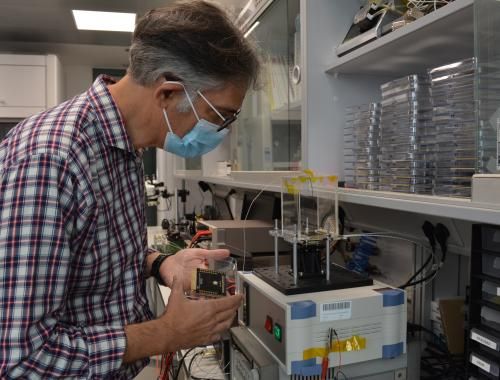
The report on energy storage talks about the new metals that are being used to obtain batteries with higher energy density and at a cheaper price. The IMB-CNM is mentioned for its research on portable devices powered by heat. These are silicon microstructures that take advantage of the ambient temperature to generate electricity and thus power low-consumption sensors.
It is a work that is carried out in the MESSI group where Luis Fonseca, a scientist of the group and current director of the institute, is involved. Fonseca declares that "this technology has two challenges", one is "to improve the thermal effectiveness of the device, that is, that the entire external thermal gradient is available for conversion by the thermoelectric material". To do this, they use printed electronics and rapid prototyping techniques.
The other challenge is to expand the range of silicon-compatible thermoelectric materials beyond nanowires, where we speak of thin layers of silicon alloys or functional oxides. "Combining silicon technologies with the integration of foreign functional materials has involved a dialogue between two different technological worlds: micronanofabrication and materials", explains Fonseca in the article.
Semiconductors to electrify the industry and decarbonize it
This report focuses on power electronics and the research carried out by the PDS group, Power Devices and Systems, which has been exploring semiconductors for more than 30 years and is the only CSIC team devoted to the field.
This branch of electronics uses materials such as silicon (Si) and more efficient derivatives to contribute to the replacement of fossil fuels. Power electronics is at the heart of wind turbines, electric cars or photovoltaic panels and is essential to take advantage of renewable energy generation.
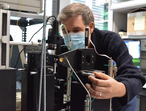
The IMB-CNM participates in a European project, iRel40, to improve the reliability and useful life of electronic components. The team investigates failure detection and degradation indicator parameters through artificial intelligence. The improvement of the predictive maintenance of the system through self-correction helps to considerably extend its life time. The short useful life of some electronic components is one of the most widespread problems in the industry, forcing their replacement and generating waste. Works in this line help to extend its life without changing the materials or the manufacturing process.
Xavier Perpiñà leads the IMB-CNM contribution to the project and declares that "the development of more compact and reliable converters will allow a rapid evolution of alternatives to fossil fuels in the field of mobility, covering urban and interurban land, air and maritime."
Power electronics has been looking for substitutes for silicon for years. This material was at the heart of the microelectronics revolution and is very abundant on Earth, although substitutes that offer more optical properties and more bandwidth to withstand higher frequencies and allow a more compact design are now being sought.
Gallium nitride (GaN) is a promising semiconductor that offers lower energy losses. It has been the central element in the transition from incandescent light bulbs (banned in the European Union since 2012) to LED lighting systems.
The problems presented by the massive implementation of this semiconductor are thermal management (cooling) and reliability. Xavier Jordà indicates that "gallium nitride HEMT transistors are the best positioned for use in very high efficiency compact power converters." These systems would be widely used in photovoltaic generation or power supplies for electronic systems.
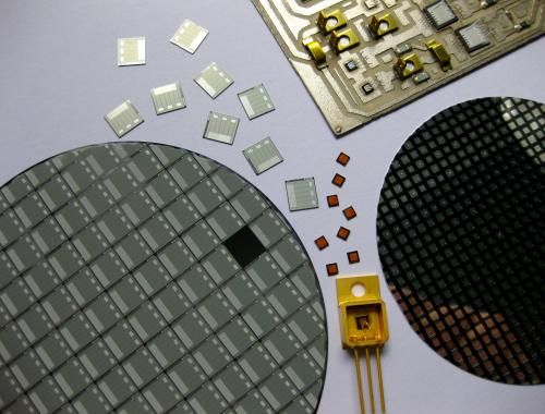
Another well-positioned semiconductor is silicon carbide (SiC), which is already used in hybrid and electric cars, rail transport and power supplies. A team from the IMB-CNM has developed MOSFET transistors (metal-oxide-semiconductor field-effect transistor) on silicon carbide substrates and high-voltage devices.
Synthetic diamond is a semiconductor that also offers better properties than silicon. The IMB-CNM has collaborated on the first high-power electronic device with diamond, within the framework of the European GreenDiamond project. The device has a MOS (metal-oxide-silicon transistor) structure in an inversion regime and the institute's participation explored new encapsulations, the cover and protection of the chip, capable of withstanding the extreme conditions of these devices.
Philippe Godignoon was the project's principal investigator: "Synthetic diamond is a bandgap semiconductor that will switch to high power and dominate energy systems for decades to come. It will withstand very high voltage and current power lines."
CSIC Clean Room: clean manufacturing
The magazine also has a foldout where you can see the Micro and Nanofabrication Clean Room of the IMB-CNM, a Singular Scientific and Technical Infrastructure, ICTS, which maintains extremely clean air to eliminate the presence of dust and particles. Air circulation, temperature and humidity are some of the parameters that are controlled in order to manufacture semiconductor devices. It is the main facility in Spain where complete integrated circuits and devices are manufactured.
- 01: Luis Fonseca in the Laboratory. IMB-CNM.
- 02: Xavier Jordà and Mariana Raya in the Power Devices and Systems Laboratory. IMB-CNM.
- 03: Xavier Perpiñà in the Thermal Characterization Laboratory. IMB-CNM.
- 04: Silicon carbide devices. IMB-CNM.


