


First meeting of the new European pilot line for the development of semiconductor-based quantum technology
IMB-CNM is participating in the European SPINS consortium for the fabrication of semiconductor-based quantum devices, which was officially launched yesterday at a meeting held at IMEC’s facilities in Belgium
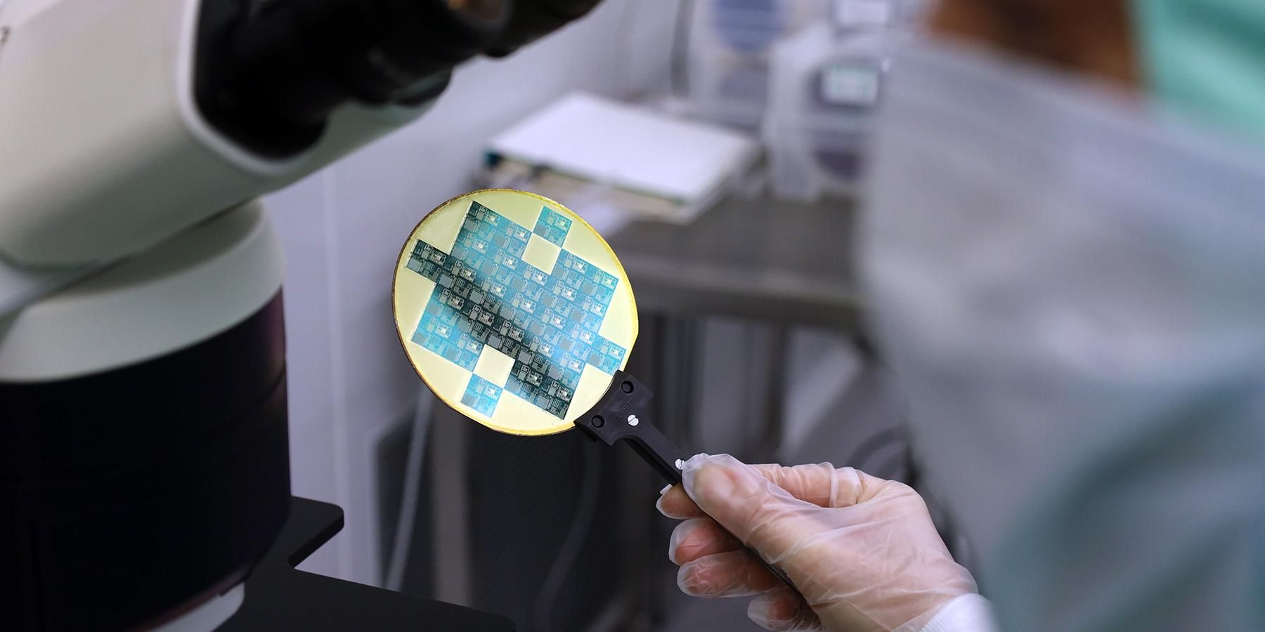
Quantum technology is a rapidly growing field of research due to its potential to revolutionize society. Through phenomena such as quantum superposition, it will enable the development of devices with capabilities that are currently unimaginable, surpassing those of conventional technology. The European Union, through initiatives to strengthen technological sovereignty under the Chips Joint Undertaking, launched a new pilot program in April to explore the potential of semiconductor-based quantum devices, known as SPINS.
The Institute of Microelectronics of Barcelona (IMB-CNM), a CSIC-affiliated center, is the Spanish research center with the greatest involvement in SPINS. The company Quantum Motion Spain and the CIC Nanogune center are the other Spanish members. Coordinated by IMEC from Belgium, the pilot line formally met for the first time yesterday, May 11, at IMEC’s headquarters in Leuven. With SPINS, the IMB-CNM officially participates in three of the pilot lines launched by the EU as part of its strategy to strengthen technological sovereignty, in addition to the two Spanish centers of excellence, and consolidates the CSIC’s role in the new European chip ecosystem.
Below we reproduce an original article from the magazine CSIC Investiga #10 Cuántica, which explores how this technology works.
Creating quantum dots using microelectronic technology
Approaches to quantum development often involve rethinking design and manufacturing methodologies, as many current systems lack the capacity to produce such devices. However, the new pilot project proposes to advance a solution that prioritizes efficiency: developing quantum technology based on semiconductors. Thus, the manufacturing methods standardized over decades by the microelectronics industry—which produces chips—could be applied to the creation of quantum devices. The IMB-CNM has a research group dedicated to this.
“We focus on the fabrication of semiconductor-based spin qubits using silicon MOS transistor technology, which is available at the IMB-CNM,” explain Francesc Pérez Murano and Joan Bausells, CSIC research professors at the IMB-CNM and leaders of this line of technological research in Spain. MOS (Metal-Oxide-Semiconductor) transistor technology is the manufacturing standard in the microelectronics industry, used to manufacture the vast majority of chips that make up computers and electronic devices.
The NEMS and Nanofabrication Group (NanoNEMS) at IMB-CNM is working on the development of platforms that combine advanced nanomanufacturing techniques to create scalable quantum devices. All of this takes place in the IMB-CNM's Micro and Nanofabrication Clean Room, where the temperature, humidity, and even the number of airborne particles are strictly controlled. In this case, it contains between 100 and 10,000 particles per cubic foot, compared to a hospital operating room, which has around 35,000, or a normal room, which typically exceeds one million.
Conditions such as temperature, pressure, and air exchange rate are kept constant to ensure that processes can be carried out identically in each circuit, since components of minute dimensions (micro- and nanoscale) are being manufactured. All of this is done to produce integrated circuits (chips), sensors, actuators, and detectors, among other devices.
Why semiconductor qubits may be the future of quantum computing
Both semiconductor and superconducting qubits can be fabricated using existing microelectronic platforms. There are also other technologies, such as trapped-ion qubits or photonic qubits, each with its own challenges and characteristics. Unlike the former, these do not necessarily use conventional microelectronic processes, as they rely on optical systems or electromagnetic fields.
Superconducting qubits are currently the most advanced in terms of practical application. However, they have a major limitation: their size. With dimensions ranging from 10 to 100 microns —very large in terms of microelectronics— integrating them into chips with thousands of qubits is complex. For this reason, technologies such as semiconductor spin qubits, which are more compact and compatible with industrial processes, are gaining prominence in the race for scalability.
For their part, spin qubits allow for more compact designs and operation under less demanding conditions. "A quantum processor with millions of semiconductor spin qubits could be integrated into a chip of standard dimensions, 10 by 10 millimeters," adds Joan Bausells.
Semiconductor spin qubits are more robust and resistant to environmental and temperature effects, precisely because the number of integrated qubits can occupy less space. As for system cooling, they can operate at 1 K, a considerably low temperature, but one that is relatively more achievable than that required by superconducting qubits. To date, the feasibility of 16 semiconductor spin qubits has been demonstrated.
Quantum computing is still in the development phase, but advances in semiconductors and nanomanufacturing are bringing us closer to the possibility of having functional quantum chips —integrating millions of qubits— in real-world applications.
Beyond abstract calculations, this technology could enable the simulation of molecular behavior in living organisms, which would facilitate the design of new personalized medical treatments or drugs. It could also be applied to optimizing logistics routes in real time, or to economic modeling by improving the ability to predict complex scenarios. It could even accelerate the training of artificial intelligence algorithms, reducing the time and resources needed to process large volumes of data.
Spin qubits allow for more compact designs and operation under less demanding conditions. "A quantum processor with millions of semiconductor spin qubits could be integrated into a chip of standard dimensions, 10 by 10 millimeters," add the researchers.

How are spin qubits manipulated and created?
Qubits, or quantum bits, are the basic unit of quantum devices and can store much more information than a classical bit. Beyond the 0 and 1 states of binary logic, a qubit can exist in a quantum superposition —that is, in a combination of both states at the same time. This property allows for exponential computing: one qubit represents two simultaneous states, two qubits represent four, and so on. Recently, IBM unveiled the Quantum System Two quantum supercomputer in San Sebastián, featuring a processor with up to 156 qubits—the first of its kind in Europe. Meanwhile, the Barcelona Supercomputing Center (BSC) houses the MareNostrum 4 supercomputer, based on superconducting qubits. The industry’s goal is to increase the capacity of supercomputers with thousands of qubits in a stable manner to perform more calculations.
In the case of semiconductor-based spin qubits, the two quantum states are due to the electron’s spin. “It is the quantum equivalent of rotation around its axis for a classical particle, but with two possible values, as if it were ‘spinning’ in opposite directions,” says Francesc Pérez-Murano about spin; whose two states “have different energies in the presence of a magnetic field.”
“We can only manipulate the qubit if we individually and precisely control the energy of a single electron.” To do this, “we need to build a ‘quantum dot,’ a kind of trap to keep the electron confined,” note researchers Jordi Llobet and Esteve Amat, from the NanoNEMS group at the IMB-CNM.
Confining the electron —which serves to trap and control the qubit— is one of the major challenges today. The point must be extremely small, as small as 30 nanometers, ten times thinner than a human hair and, therefore, imperceptible to the human eye, so that quantum effects manifest and the electron’s energy states are discrete, meaning they can be separated from one another.
"By applying a magnetic field, the electron’s energy state will split into the two separate spin states that form the qubit,” they add. To distinguish this separation, operations must be conducted at extremely low temperatures, at or below 1 Kelvin (equivalent to -272°C).
How does the IMB-CNM attempt to “construct” this quantum dot? Through nanoelectrodes: “Nanoelectrodes allow us to confine the electron using electrical voltages, adjusting the size and the ‘depth’ of the dot in terms of energy,” explains Marta Fernández-Regúlez, another researcher in the group. An electrode is a component that allows electrical voltages to be applied within a system to control the behavior of particles such as electrons. In the case of nanoelectrodes, they enable manipulation at the quantum scale.
The research team proposes using nanoelectrodes to adjust the "barrier" separating the electrons and allow interaction between them by applying electrical voltages. To achieve this, many electrodes are needed in a very small space, so “a more refined design is needed that leaves a little more room for the components," says Marta Fernández. Throughout this process, the experience and expertise accumulated in conventional microelectronics processes come into play.
But what are these dimensions? A quantum dot can measure about 30 by 30 nanometers—or even less—much smaller, for example, than a human cell. To achieve this configuration, at least three electrodes are needed: one at the center of the quantum dot and two as lateral barriers. Creating the qubit requires positioning each of these quantum dots with great precision. Ensuring that all the dots are identical is extremely complicated, given their tiny size, which impacts the reliability of the devices.
“These dimensions require extremely advanced and precise processes, comparable to those used to manufacture transistors in 5- or 3-nanometer chips, the latter being the smallest size the industry has achieved,” notes Joan Bausells.
Manufacturing in the Micro and Nanofabrication Clean Room
“The need to manufacture miniature qubits is both an advantage and a challenge,” they add. In the IMB-CNM Clean Room, the main hub of the Micronanofabs Unique Science and Technology Infrastructure (ICTS), they are used to manufacturing micron-scale integrated circuits—skills that are now also being applied to “build” quantum wells. However, the scale and the need to replicate the processes remain complex.
Semiconductor spin qubits are fabricated using silicon technology, sometimes combined with thin layers of germanium or silicon-germanium heterostructures. Their fabrication builds on decades of advancements in the microelectronics industry, which have now enabled the transistors that make up computer and mobile phone chips to have critical dimensions of just a few atoms.
Integrated circuit technology is characterized by its high performance and reliability, enabling a scaling that will, in the future, help make quantum processors composed of millions of qubits a reality. However, greater control over manufacturing processes is still needed to achieve high-quality qubits.
In this context, the IMB-CNM Clean Room participates in several European-level initiatives aimed at advancing manufacturing technology. With the goal of defining quantum dots using nanoscale electrodes, the IMB-CNM participates in two European projects (Qu-Pilot and the aforementioned SPINS), in coordination with leading European R&D institutions in microelectronics (IMEC, CEA -Leti, and VTT, among others), where pilot manufacturing lines are being established to provide the first silicon quantum processors for European companies.
On the other hand, in a more exploratory direction—but one with greater potential for producing high-quality qubits—research is underway into the possibility of creating devices in which the quantum dot is defined by a single atom. The challenge here is to position the atom at a specific location and with sufficient precision to make industrial-scale manufacturing practical. This effort combines the capabilities of the IMB-CNM with new processes being developed at the Swiss Federal Institute of Technology in Lausanne (EPFL) as part of the SiDoQu project.
Confining the electron —which serves to trap and control the qubit— is one of the major challenges today. The point must be extremely small, as small as 30 nanometers, ten times thinner than a human hair and, therefore, imperceptible to the human eye, so that quantum effects manifest and the electron’s energy states are discrete, meaning they can be separated from one another.


