


CSIC participates in the new European pilot line to lead the advanced packaging and heterogeneous integration for electronic components
CSIC's Institute of Microelectronics of Barcelona (IMB-CNM-CSIC) is the only Spanish institution within the consortium, which aims to strengthen European technological resilience by improving semiconductor supply chains. With more than 730 million euros over the next four and a half years, the Advanced Packaging and Heterogeneous Integration for Electronic Components and Systems is one of the largest pilot lines funded by the Chips Joint Undertaking (Chips JU) and national funding authorities of Austria, Belgium, Finland, France, Germany, Greece, Portugal, Spain, through the “Chips for Europe” initiative
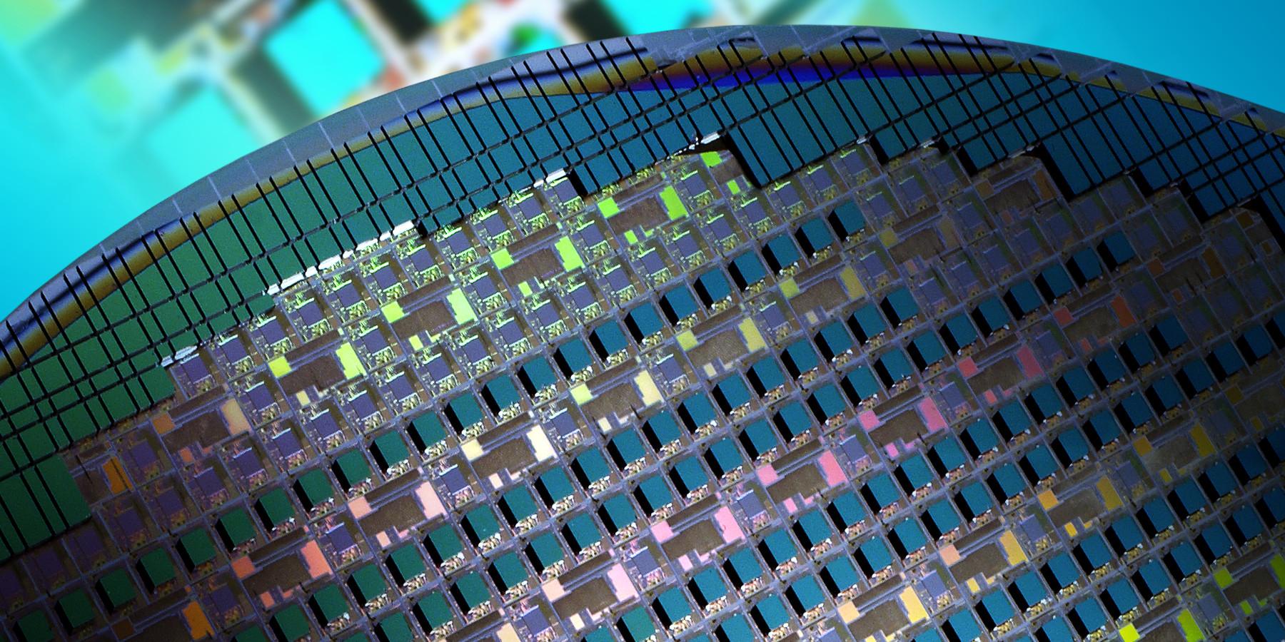
Main image: Processed wafer from Fraunhofer ISIT. APECS.
The pilot line for “Advanced Packaging and Heterogeneous Integration for Electronic Components and Systems” (APECS) is a major leap forward in strengthening Europe's semiconductor manufacturing capabilities and chiplet innovation as part of the European Chips Act. The CSIC’s Institute of Microelectronics of Barcelona (IMB-CNM-CSIC) is the only Spanish institution within the consortium, adding its expertise in design, fabrication and packaging, as well as the capabilities of its Micro and Nanofabrication Clean Room, the largest in Spain.
APECS is one of the five pilot lines, approved or in negotiation, and funded by the Chips Joint Undertaking (Chips JU). Coordinated from Germany by the Fraunhofer-Gesellschaft and implemented by the Research Fab Microelectronics Germany (FMD), the consortium will establish a solid foundation for resilient and robust European semiconductor supply chains by providing large industry players, SMEs and start-ups with facilitated access to cutting-edge technology.
Total funding for APECS amounts to € 730 million over four and a half years. More than half of it comes from the Chips JU and the other amount is provided by the national funding authorities of Spain, Austria, Belgium, Finland, France, Germany, Greece and Portugal through the “Chips for Europe” initiative.
The IMB-CNM-CSIC contribution focuses on integrated microchannel cooling technologies, through researcher Miguel Ullán, and on the design and additive manufacturing of antennas, with researcher Eloi Ramon.
Emerging technologies in advanced integration
The consortium's goal is to bridge the gap between application-oriented research and innovative developments in heterogeneous integration, in particular emerging chiplet technologies, where each chip subsystem is manufactured separately at the most convenient technology node and then functionally assembled with the rest. This independent production simplifies technological processes, optimizes performance and lowers costs. By going beyond conventional approaches, APECS will offer robust and reliable heterogeneous systems, which will significantly boost the innovation capacity of the European semiconductor industry.
The heterogeneous integration of chips with diverse origins and functionalities in an advanced package is essential to obtain complex intelligent systems with the smallest possible size and at a reasonable cost, as it enables the incorporation of more functionalities and capabilities to increase the production yield. Large companies and technology development centers around the world are already incorporating these innovations in the most advanced systems, such as computers, cell phones or automotive electronics.
The director of the IMB-CNM-CSIC, Luis Fonseca, clarifies that “this is a high value-added domain in which Europe is not technologically behind other regions of the world and in which its contribution can be leading”, unlike other regions in the world.
APECS will play a key role in supporting European microelectronics by developing new system integration technologies and unlocking new functionalities within the system technology co-optimization (STCO) approach. This will enable European companies to develop advanced products, even in low quantities, at competitive costs. By providing a wide range of technologies on a single platform, APECS is positioned to become Europe's leading hub for the development of advanced packaging and heterogeneous integration.
It will be a key driver of collaboration between European research centers (RTOs), industry and academia, fostering a dynamic innovation ecosystem. Users will benefit from a single point of contact to the APECS pilot line. It will cover end-to-end design and pilot production capabilities and accelerate progress from cutting-edge research to practical and scalable manufacturing solutions.
IMB-CNM participation in the consortium
IMB-CNM-CSIC brings advanced manufacturing capabilities and expertise in the development of microelectronic technologies. One of the goals of its contribution is “the development of novel cooling technologies for the integration of ASICs (integrated circuits with a specific application) and image or radiation sensors,” says Miguel Ullán.
“We intend to work on two approaches, depending on whether the evacuation of high heat densities is required, as in the case of ASICs, or whether what is sought is a homogeneous temperature distribution, more applicable to the case of image and radiation sensors. All this with the aim of incorporating cooling along with other functionalities in the heterogeneous integration of systems,” adds Ullán.
In turn, the institute will apply its experience in additive manufacturing and heterogeneous integration together with knowledge in the use of sustainable materials to minimize their ecological footprint. The aim is to “achieve the heterogeneous integration of sustainable systems with structural resolutions of less than 50 microns and enable the direct integration of electronic components by means of microelectronic assembly as part of the additive manufacturing process,” says Eloi Ramon. All this will result in “greater design freedom, including the creation of combined circuits with 3D substrates,” he adds.
To do so, the institute will be responsible for the “development of high-resolution additive manufacturing technologies for high-frequency electronic applications, such as 5G, 6G, millimeter-wave (mm-Wave) and sub-THz applications. Along with the development of a hybrid manufacturing process for the production of free-form structural electronics, including the ability to directly integrate electronic components such as printed antennas, chips or SMD components,” Ramon concludes about its contribution.
By providing a wide range of technologies on a single platform, APECS is positioned to become Europe's leading hub for the development of advanced packaging and heterogeneous integration.
The only Spanish institution with presence in two Chips JU pilot lines
Chips JU aims to improve Europe's technological resilience, secure supply and value chains and drive innovation in emerging fields such as energy-efficient artificial intelligence, manufacturing, mobility, information and communications, neuromorphic and quantum computing, as well as reliable and sustainable electronics.
APECS is one of the two pilot lines in which IMB-CNM-CSIC participates in addition to PIXEurope, dedicated to integrated photonic circuits and coordinated by the Institute of Photonic Sciences (ICFO) at the continental level.
IMB-CNM-CSIC is the only Spanish institution with such a presence in Chips JU, as it is also part of the two shortlisted proposals to establish two competence centers in Spain. These are PIXSpain CC, focused on integrated photonics, and MicroNanoSpain, dedicated to microelectronics design and manufacturing. They are centers with European and national funding to operate for four years. With nearly one million euros per year, the funds will be used to organize the network of institutions that comprise them, provide support staff and partially subsidize external access to services, thus strengthening their respective ecosystems.
About the Chips Joint Undertaking (JU)
The European Commission's Chips Joint Undertaking supports research, development, innovation and future manufacturing capabilities in the European semiconductor ecosystem. It was launched by EU Council Regulation No. 2021/1085 and amended in September 2023 as part of the Chips for Europe initiative. To address the semiconductor shortage and strengthen Europe's digital autonomy, it has significant EU, national/regional and private industry funding of nearly €11 billion. Chips JU is funded by the European Union, participating states and private members.