


Innovative IMB-CNM method enables semiconductor qubit fabrication using standard microelectronics processes
A new method developed by researchers at IMB-CNM allows for high-precision, low-cost fabrication of semiconductor qubits, paving the way for industrial-scale quantum computing
Researchers at the Institute of Microelectronics of Barcelona (IMB-CNM-CSIC) have developed an innovative method for fabricating semiconductor qubits. Currently under evaluation for a European patent, the breakthrough introduces a fabrication technique compatible with standard semiconductor industry processes — a key step toward the large-scale integration needed for quantum computing to reach its full potential.
Quantum computing is expected to handle challenges that remain out of reach for even the most advanced classical systems. And that relies on the qubit, the fundamental unit of quantum computation. Unlike classical bits, which can represent a 0 or a 1, qubits can exist simultaneously in multiple states thanks to quantum mechanical properties like superposition. This allows quantum processors to handle vast amounts of information in parallel, opening doors to advancements in fields such as chemical simulations, novel materials discovery, and financial optimization.
To realize this promise, experts estimate that quantum computers will need tens of thousands of qubits. State-of-the-art machines currently only reach a few hundred. Achieving higher integration densities is critical, and semiconductor-based qubits are a promising solution.
Compared to other technologies, such as superconducting qubits, semiconductor qubits are nanometric rather than millimetric in scale and can be manufactured using widely adopted materials like silicon or germanium. These are already standard in the electronics industry, making semiconductor qubits a strong candidate for scalable quantum processors built with existing infrastructure.
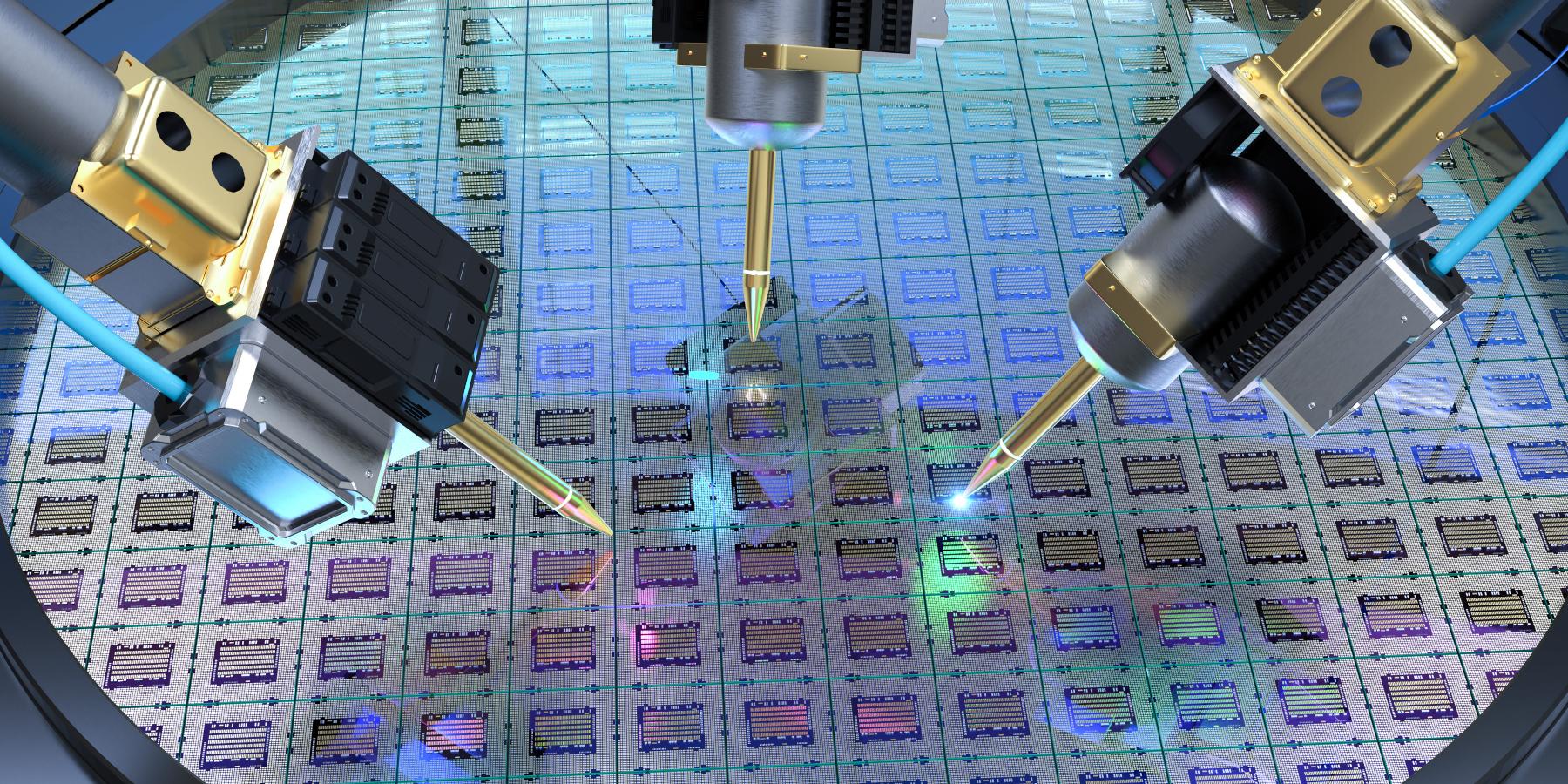
In this context, a team from the Nanofabrication and Nanomechanical Systems Group at IMB-CNM, led by researchers Marta Fernández, Joan Bausells, and Francesc Pérez-Murano, has developed a new fabrication process based on CMOS (complementary metal–oxide–semiconductor) technology. This process achieves nanometer-scale resolution by combining advanced top-down and bottom-up nanofabrication techniques.
Specifically, the method integrates electron beam lithography with directed self-assembly (DSA) of block copolymers (BCPs) — materials made of two distinct polymer chains that spontaneously organize into well-defined nanoscale patterns, such as lines or dots. By using lithographic guides, researchers can direct this DSA to form structures on a chip with high precision. One of the BCPs is then selectively removed, and the remaining block acts as a mask for pattern transfer onto the substrate. This process achieves sub-10-nanometer precision, essential for qubit fabrication, offering a cost-effective and scalable alternative to conventional high-resolution techniques like extreme ultraviolet (EUV) lithography, which rely on expensive, complex equipment.
"This is a precise, affordable, and scalable qubit fabrication process that is fully compatible with the semiconductor industry of today," says Marta Fernández.
The work is part of the Pilot4QTech project and framed within major European initiatives such as QuPilot (Supporting Experimental Capabilities for Quantum Technologies), which includes key nanoelectronics centers like IMEC, CEA-LETI, and VTT. It also supports projects SiDoQu (Nanopatterning and Polymeric Precision Doping: towards single dopant quantum devices) and DoNQu (Deterministic Doping for Nanoelectronics and Quantum Devices), bringing together institutions such as EPFL, University of Basel, CNR, Università del Piemonte Orientale, and Imperial College London. Additionally, it is supported by QuantumTech funded by the Spanish Ministry of Science, Innovation, and Universities.
With this innovation, IMB-CNM takes a decisive step toward the future of computing, helping bring the promise of quantum technology closer to real-world applications in addressing the grand scientific challenges of the 21st century. The advance will also be part of the newly approved European pilot line for semiconductor-based quantum processors.
This initiative is framed within the CSIC Quantum Technologies Platform, a research ecosystem involving over 40 research groups.
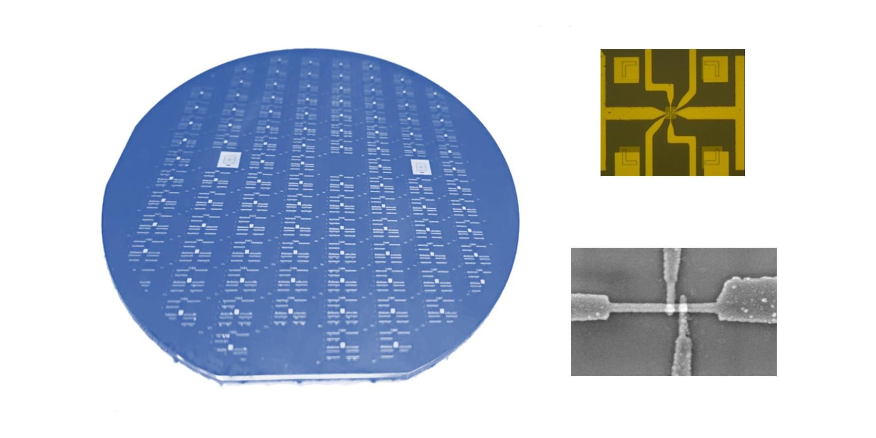
Left: processed wafer with semiconductor qubits. Right: Details of the circuit.