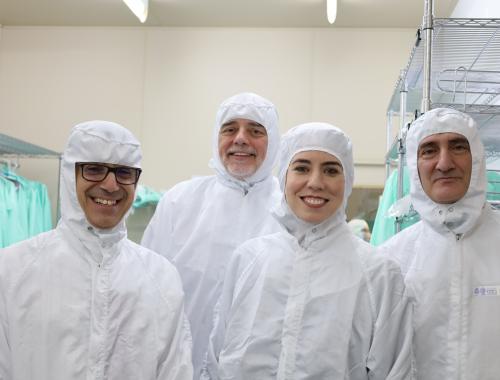
Diana Morant visits the largest research clean room in Spain at the Institute of Microelectronics of Barcelona
The Institute of Microelectronics of Barcelona will receive 25 million euros to improve its infrastructure. The project includes, among other actions, the creation of a level 2 Bioelectronics Clean Room to evaluate electronic devices under biomedical conditions.

From left to right: Xavier Jordà, Scientific Deputy Director; Mar Álvarez, Scientific Deputy Director; David Quirion, Director of the Clean Room; Luis Calvo, Institutional Delegate of the CSIC in Catalonia; Luis Fonseca, Director of IMB-CNM; Diana Morant, Minister of Science, Innovation and Universities; José María Martell, Vice President of Scientific and Technical Research at CSIC; Javier Lafuente, Rector of the Universitat Autònoma de Barcelona (UAB); Teresa Riesgo, Secretary General for Innovation; and María del Carmen Porto, Managing director of IMB-CNM.
The Institute of Microelectronics of Barcelona - National Center for Microelectronics (IMB-CNM), part of the Spanish National Research Council (CSIC), will receive €25 million in funding to improve its infrastructure and equipment. This was highlighted today by the Minister of Science, Innovation and Universities (MICIU), Diana Morant, during her visit this Thursday to the Micro and Nanofabrication Clean Room at IMB-CNM, the largest clean room dedicated to research in Spain.
"The Spanish government is investing €25 million in this center, much of it through Next Generation funds, to improve strategic autonomy," Morant emphasized.
Specifically, the Clean Room improvement project includes actions to update equipment and systems to enhance energy efficiency and research capacity. These actions include the acquisition of a new scanning electron microscope and a confocal microscope; the creation of a level 2 Bioelectronics Clean Room inside the facilities, allowing the evaluation of electronic devices in biomedical conditions, accelerating their development and clinical application; and the renovation of infrastructure, such as cooling machines, air conditioning units, and deionized water plants, which are essential to maintain working conditions and reduce energy costs.
The expansion of the facilities, adding approximately 500 m2 useful to the existing 1.500 m2, will significantly increase the technological capabilities of the Clean Room. "With this, we will continue advancing in micro and nanoelectronics, integrated photonics, and quantum technologies, which are shaping the technological future in the semiconductor field, keeping IMB-CNM as a reference point in the Spanish ecosystem and as one of its key elements in Europe. We aim to strengthen support for deeptech start-ups that require these technologies by temporarily providing them with spaces, and support for practical training activities in micro and nanotechnologies," emphasized Luis Fonseca, Director of IMB-CNM.
The IMB, which is celebrating its 40th anniversary this year and is recognized as a María de Maeztu Excellence Unit by MICIU, is part of the National Center for Microelectronics (CNM), along with the Institute of Microelectronics of Seville (IMSE-CNM) and the Institute of Micro and Nanotechnology of Madrid (IMN-CNM). IMB is the largest of the three institutes.
The Clean Room at IMB-CNM is the largest node of the Unique Science and Technology Infrastructures (ICTS) MICRONANOFABS, one of 29 ICTS in Spain, which combines the capacities and facilities of the three participating partners: SBCSIC-CNM, the Institute for Optoelectronic Systems and Microtechnology (ISOM-UPM), and the Nanophotonics Technology Center (NTC-UPV). This infrastructure provides high-value scientific support and an enhanced technological offering with open access to the national and international community of public and private R&D&I entities.
Devices with Multiple Applications
The work carried out by IMB-CNM researchers in the Clean Room has led to the development of devices with multiple applications. Among them devices in orbit around Earth in the OneWeb satellite constellation, as well as protecting solar panels in space missions to the Sun, Mercury, and Jupiter; also radiation sensors deployed in high-energy experiments at CERN.
The microelectronic devices also have medical applications, such as intracranial probes for neurodiagnostics and stimulation, or microdosimeters for innovative radiological technologies in cancer treatment; devices capable of entering living cells to help understand cellular mechanisms and support life sciences research; environmental applications, such as miniaturized sensors for air and water quality monitoring, as well as early wildfire detection. In power electronics, contributes to industrial and mobility electrification to reduce fossil fuel consumption.


