Equipment and processes of the Nanolithography Area
The Nanolithography Area is devoted to the definition of features at the submicron resolution level, and the characterization of materials, processes and devices fabricated at the institute at the nanoscale.
Techniques
- Electron beam lithography (EBL)
- AFM based nanofabrication
- Nanoimprint lithography
- Focused Ion Beam (FIB)
- Scanning Electron Microscopy (SEM)
- Resist Processing
- Optical Microcope (OM)
Equipment
AFM microscope
Bruker Icon AFM
- Close-loop scanner
- Sample size up to a 150 mm wafer
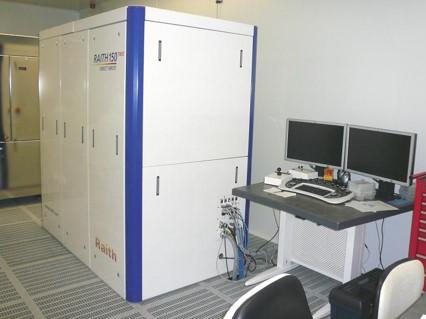
Electron beam lithography
RAITH 150 (TWO) dedicated electron beam lithography system
- From samples up to 150 mm wafers
- 0,1 to 30kV acceleration voltage
- Height Sensor
- Interferometric Stage
Nanoimprint lithography (NIL)
Obducat thermal nanoimprint system
- Sample size up to 150 mm wafers
- Maximum pressure: 80 bars and temperature up to 350 ºC
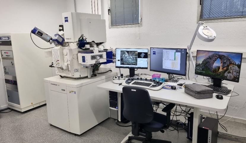
Focused Ion Beam
Zeiss Crossbeam 550L
- Sample size up to a 150 mm wafer
- Circuit editing capability
- Nanomachining capabilities
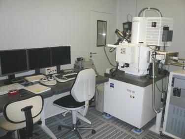
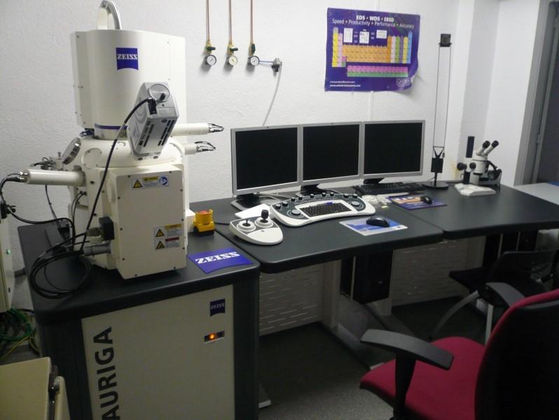
Scanning Electron Microscopy
Zeiss 1560 and Zeiss AURIGA 40 Field Emission SEMs
- 4” full acces (6 and 8 inch possible)
- EDS Oxford Detector
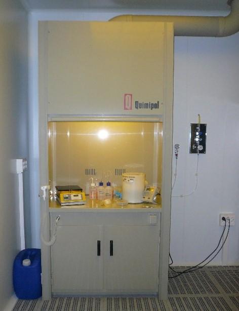
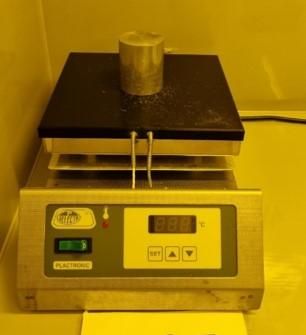
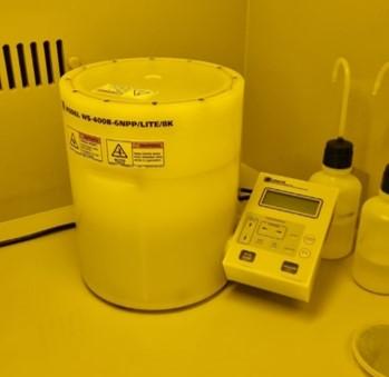
Resist Processing
Fume Hood with Laurell Spinner and Hot-Plate
- Small pieces to 6” wafers
- Hot-Plate up to 200ºC
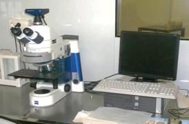
Optical Microscopy
Zeiss AxioM1
- Manual Plate
- Bright Field and Dark Field
Available Capabilities
EBL nanolithography
- Lithography on positive and negative resists
- Resolution below 20 nm
- Up to 6 inch wafers in stich fields, stitch resolution below 20nm
- Mix & Match with Optical Lithography
Nanoimprint lithography
- Imprinting of polymer resists on different surfaces.
- Imprinting of polymers foils (hot-embossing)
- Resolution below 100 nm
- Imprinting area up to 4"
- "In house" technology for mould fabrication and conditioning
Focused Ion Beam (FIB)
- Nanofabrication (Ga ions): Resolution below 20 nm depending on the material.
- Gas Injection System (GIS): Pt, C, W, TEOS deposition & O2, F etching
- Omniprobe for lamella preparation.
- SmartFIB patterning software
Characterization Capabilities
Topographical characterization by AFM
- Maximum sample size: 6'' wafer
- Maximum range of images: 30 μm (X) x 30 μm (Y) x 4 μm (Z)
- Lateral resolution (depending on surface features): 1 nm
- Vertical resolution: 0.1 nm AFM
- Other SPM techniques available on request
SEM characterization
- SEM characterisation of whole wafers up to 6''
- In-Lens, SE, EBS, STEM and BSE detectors
- Oxford EDS detectors
- Metrology (automatic large area imaging) and measuring
FIB characterization
- FIB cross-sectioning
- TEM lamela preparation
- Circuit Editing.
- SEM & FIB 3DMapping (topographic and/or EDS)
Optical MicroscopyLocal electrical characterization
- Camera and computer attached
- Multiple Objectives (x5,x10,x20,x50,x100 plus condensers)
- Bright Field and Dark Field
Download the techniques and capabilities of the Nanolithography Area
Check the Nanolithography Area
Nanolithography Team
- Xavier Borrisé (ext. 435564)
- Llibertad Solé (ext. 435557)
- Albert Guerrero (ext. 435562)