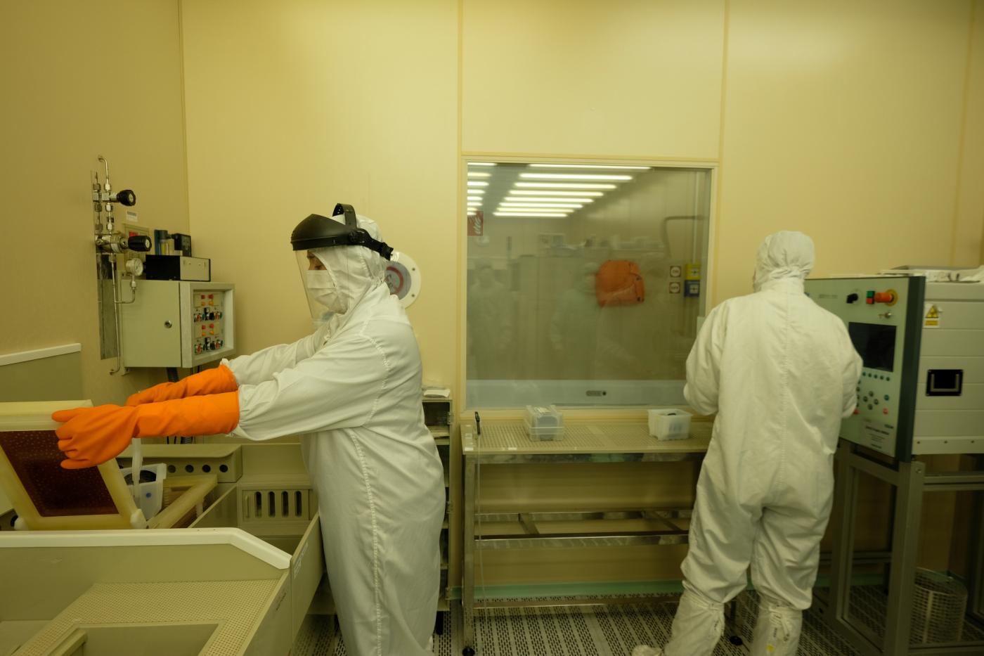
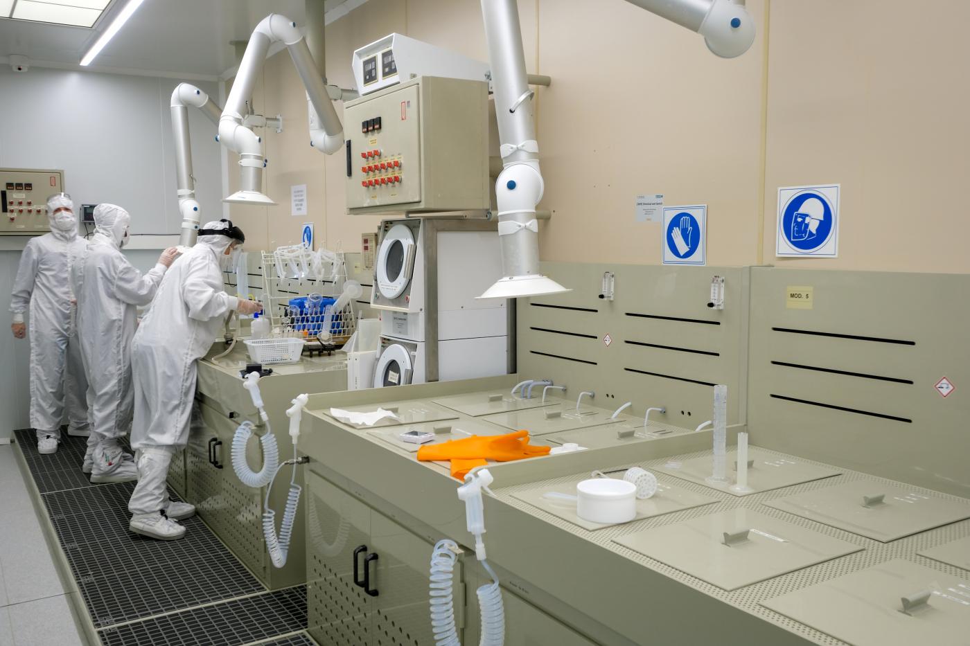
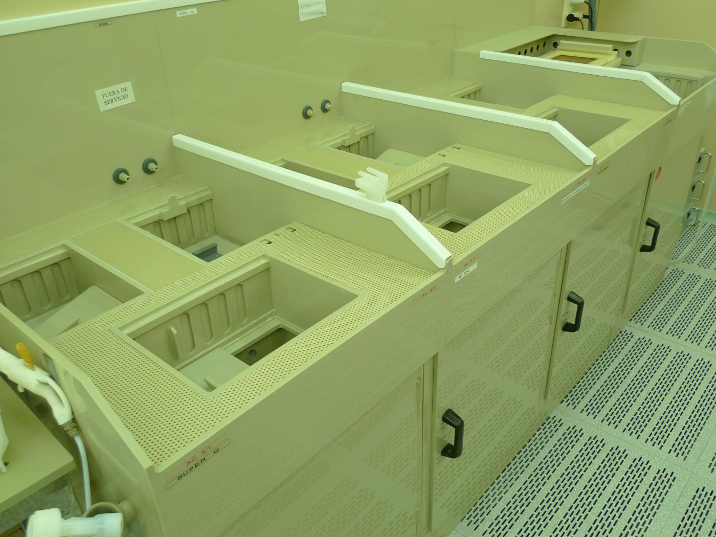
Equipment and processes of the Wet Etching and Surface Cleaning Processes Area
The Wet Etching and Cleaning Surface Cleaning Processes Area is the area where basic techniques such as metal and dielectric wet etching, surface cleaning or photoresist stripping are performed.
Techniques
- Metal and dielectric wet (isotropic) etching.
- Surface cleaning.
- Photoresist stripping: oxygen plasma and wet stripping
Equipment
Metal and dielectric wet (isotropic) etching
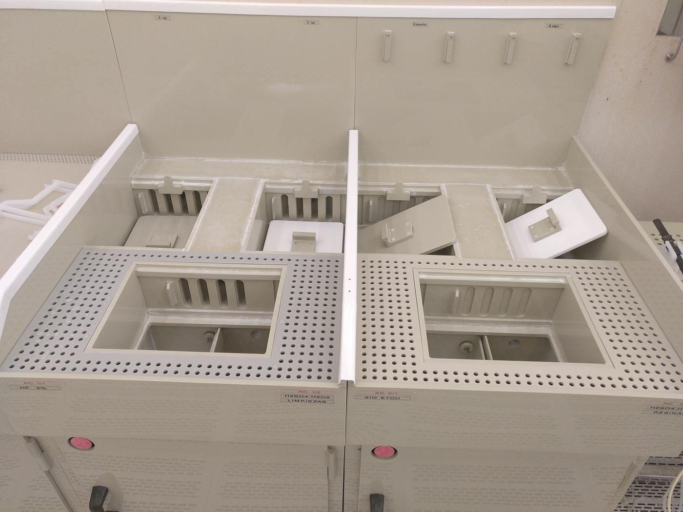
- 9 baths and 6 DI water overflow rinse tanks for CMOS compatible wafers up to 150 mm.
- 7 baths and 2 DI water overflow rinse tanks for wafers with contaminant metals up to 150 mm.
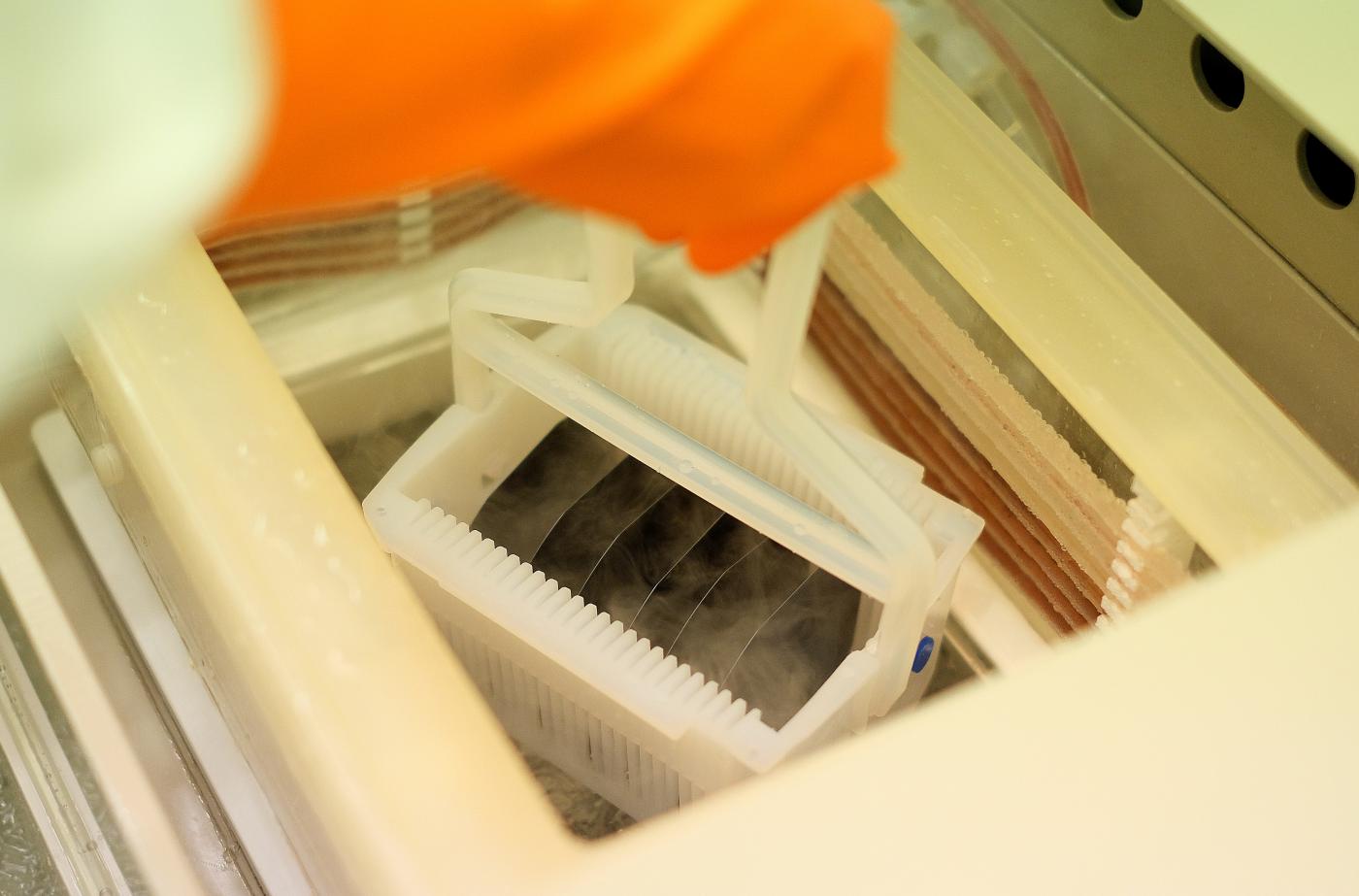
- 2 Rinse and Dryer (R&D) devoted to CMOS compatible wafers of 100 mm and 1 R&D for 150 mm wafers.
- 1 R&D for wafers with contaminant metals of 100 mm and 1 R&D for 150mm.
- 2 ovens for drying and photoresist bakes for CMOS compatible wafers and 1 oven for drying and photoresist bakes for contaminant metal wafers.
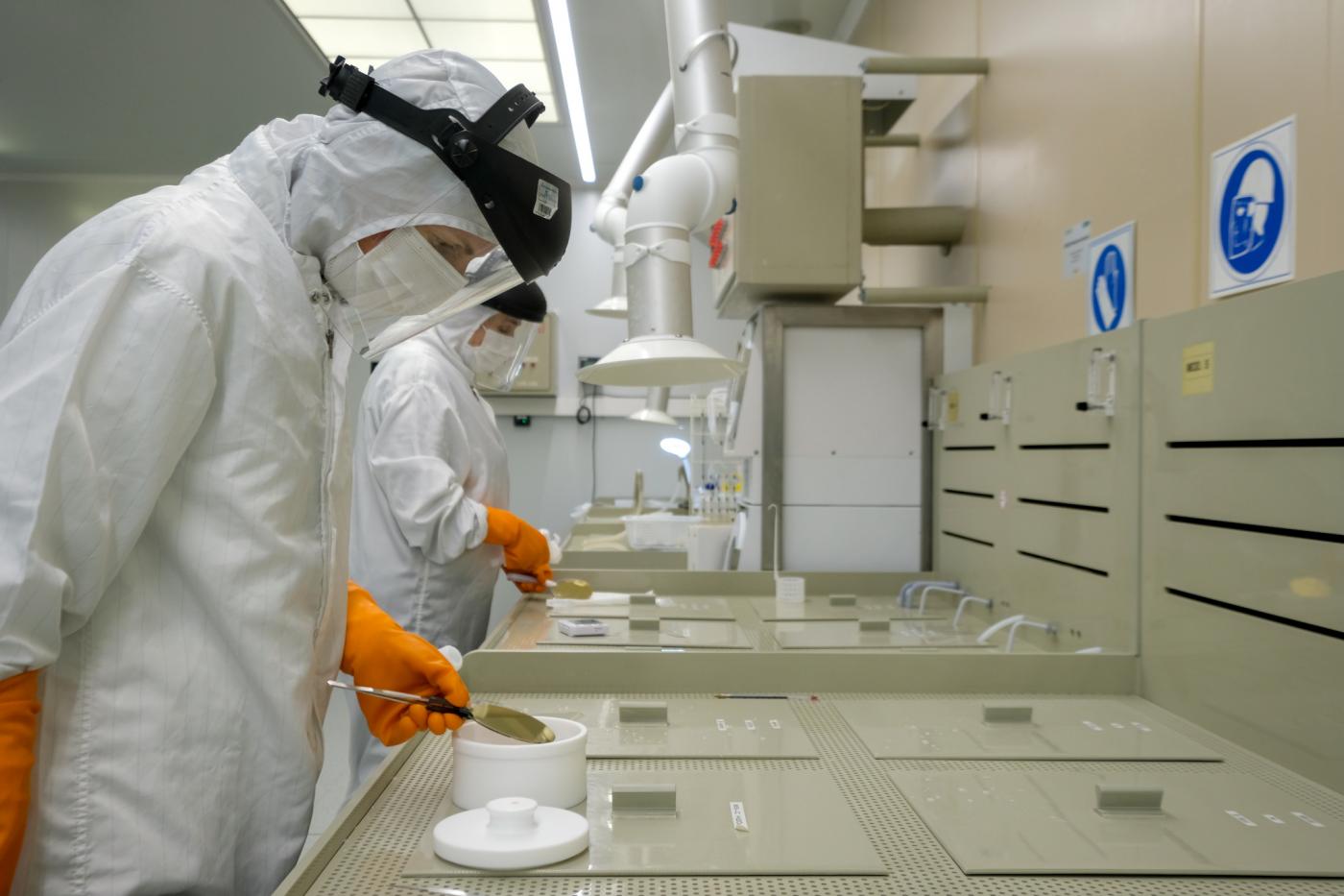
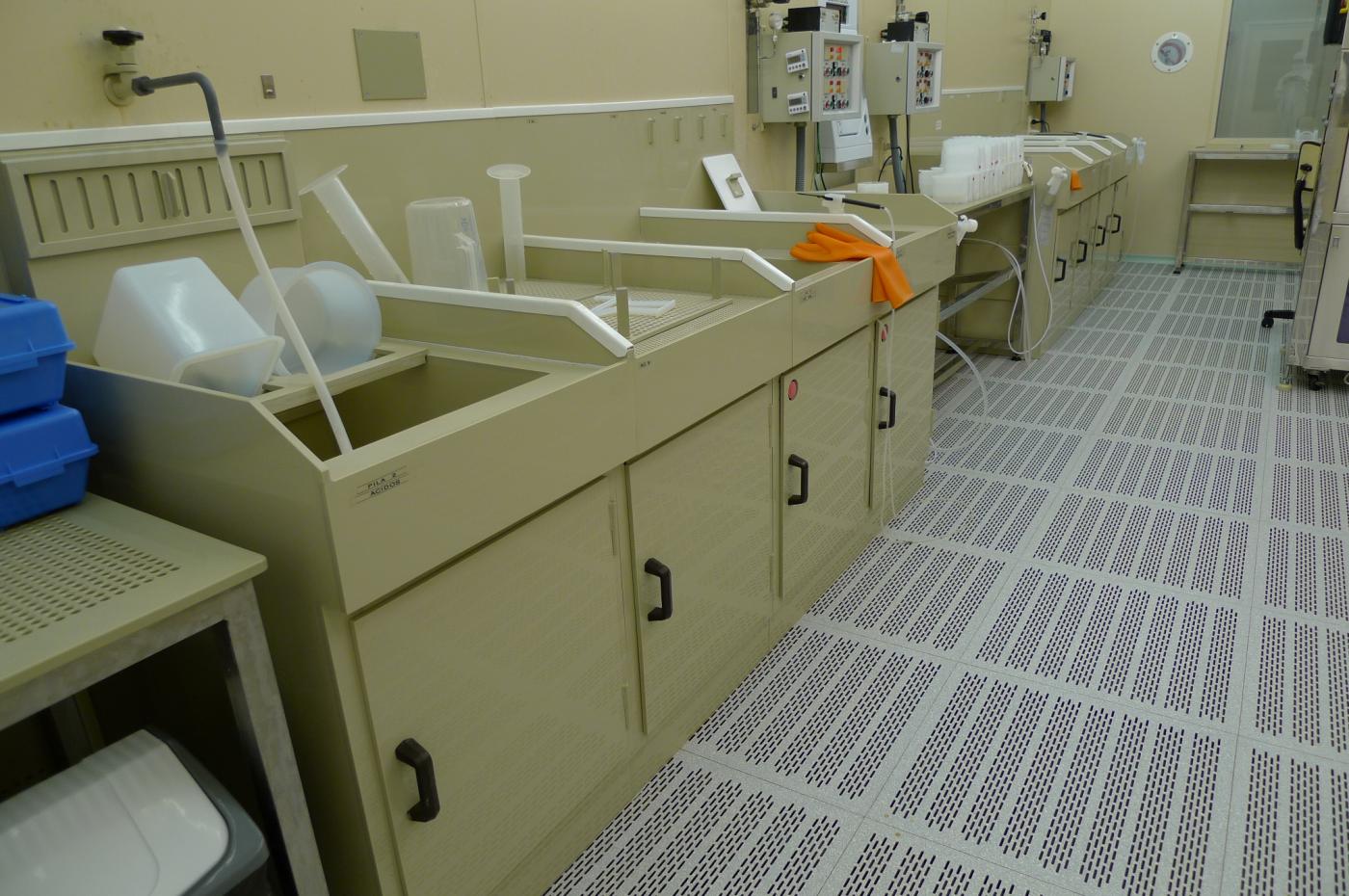
Surface cleaning
- 5 baths and 3 DI water overflow rinse tanks for CMOS compatible wafers up to 150 mm.
- 2 baths and 1 DI water overflow rinse tanks for wafers with contaminant metals up to 150 mm.
- 2 R&D (one for CMOS compatible wafers and another for wafers with contaminant metals) for 100 mm wafers.
- 2 R&D (one for CMOS compatible wafers and another for wafers with contaminant metals) for 150 mm wafers.
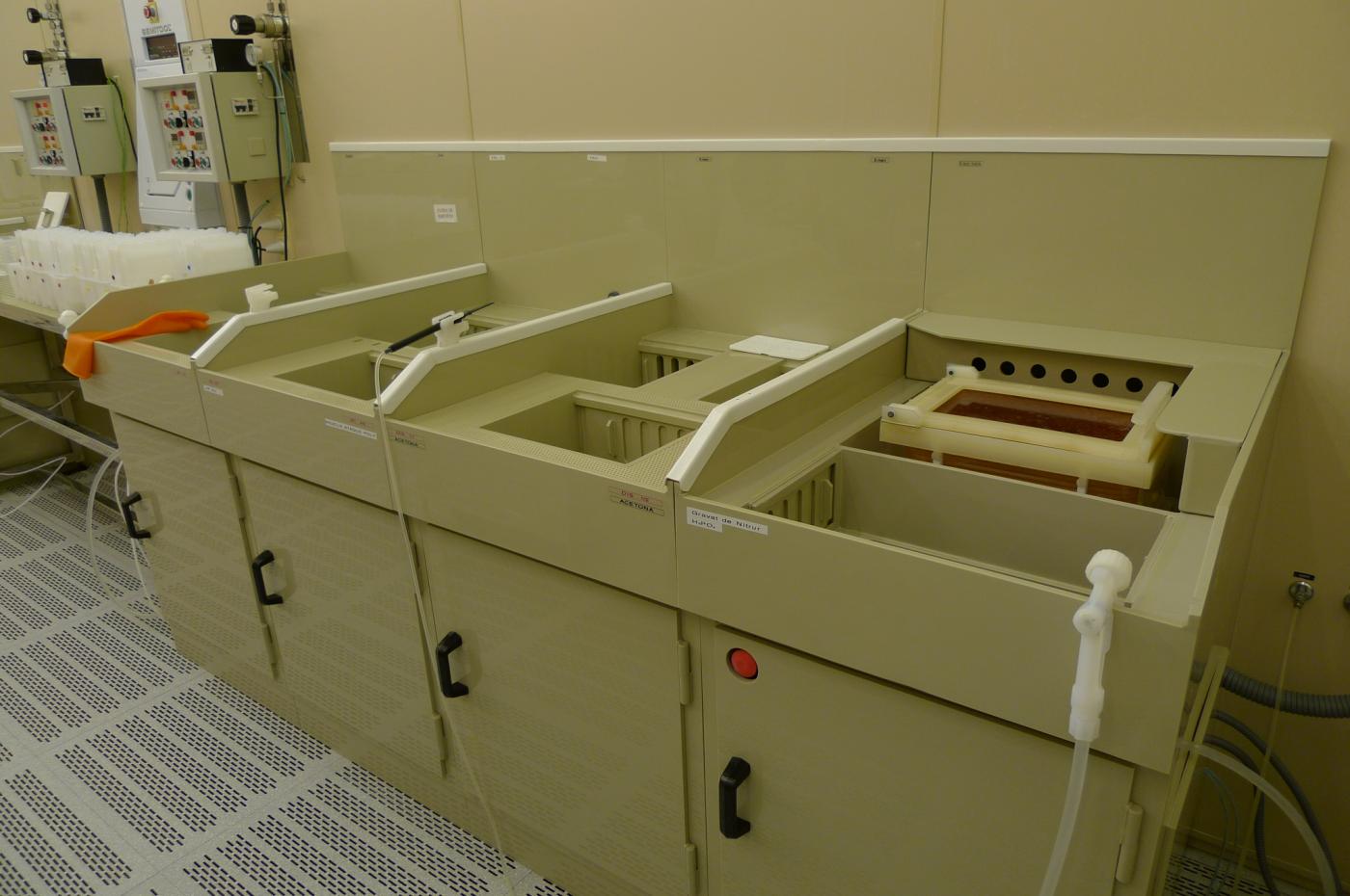
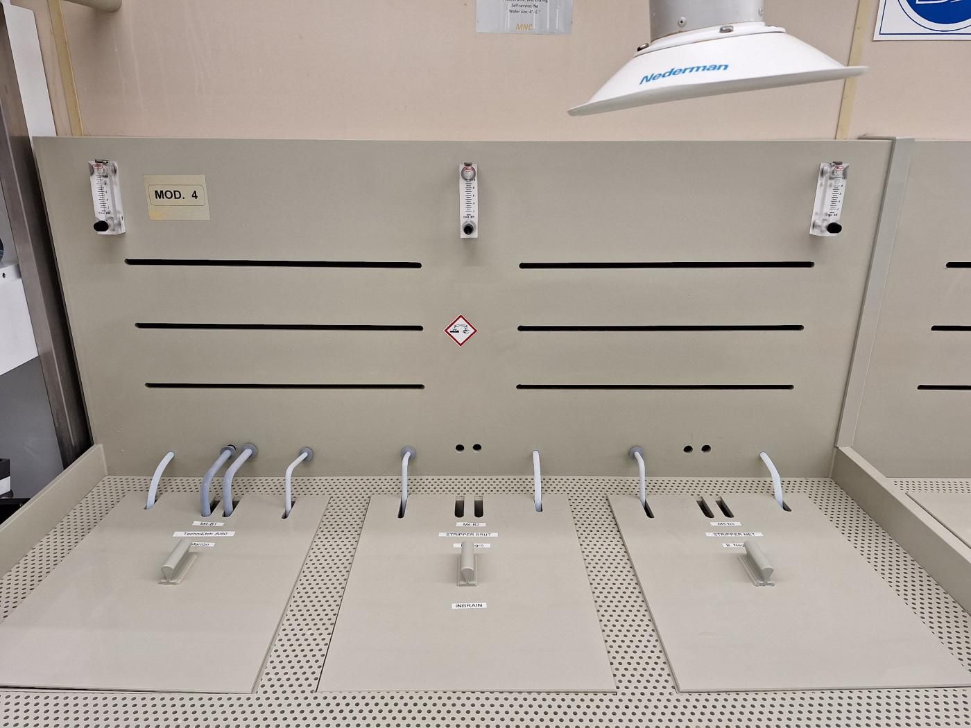
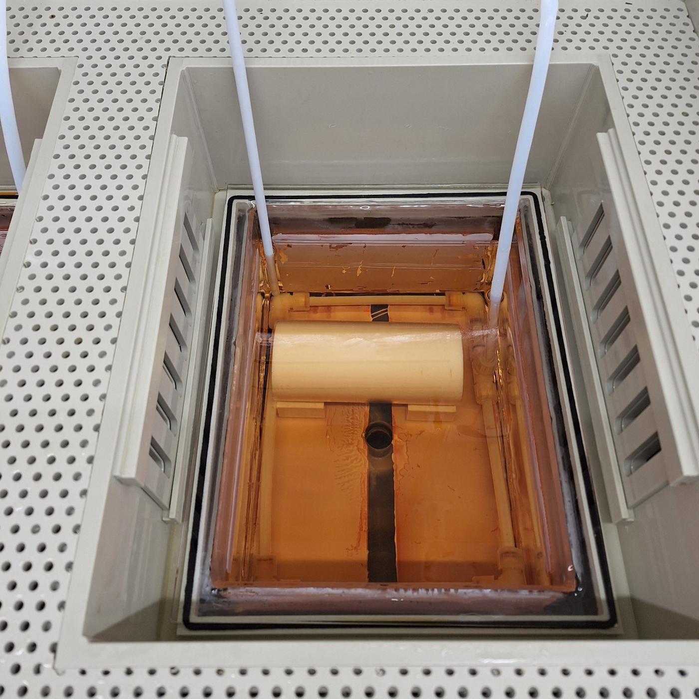
Photoresist stripping: oxygen plasma and wet stripping
- 1 double ultrasonic bath for solvents and 1 DI water overflow rinse tank for CMOS compatible wafers.
- 1 bath for wet photoresist stripping in acid and 1 DI water overflow rinse tank for CMOS compatible wafers.
- 2 baths for wet photoresist stripping for wafers with contaminant metals and 1 DI water overflow rinse tank for wafers with contaminant metals up to 150 mm.
- PVA Tepla 300SA plasma asher for photoresist stripping with oxygen plasma for CMOS compatible wafers.
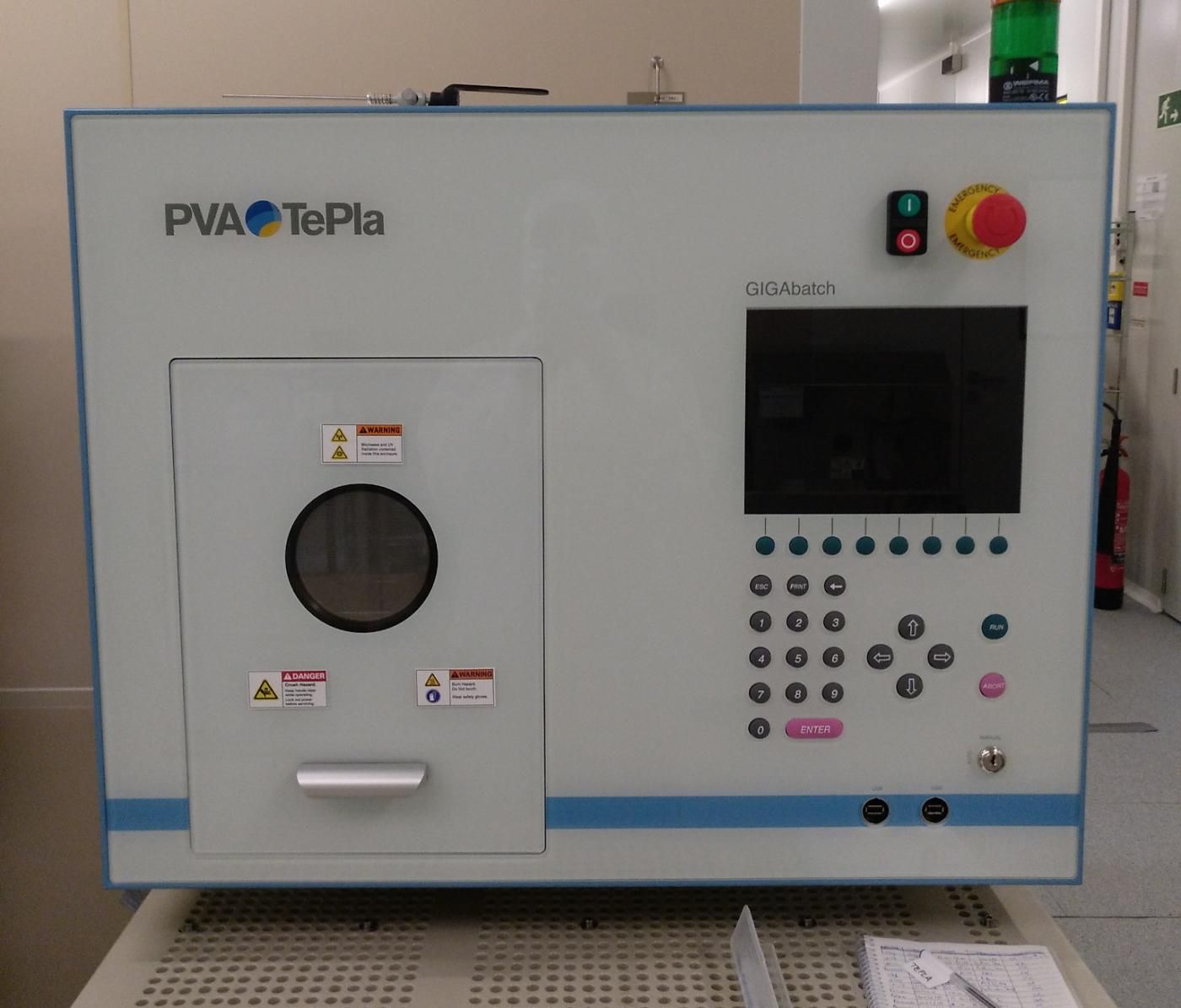
- Tepla GIGABatch 360M plasma asher for photoresist stripping with oxygen plasma for wafers with contaminant metals up to 150mm.
Available capabilities
Etching and stripping of dielectrics
- Etching and stripping of SiO2 in HF mixtures of different concentrations.
- Isotropic etching and stripping of silicon and polysilicon based on mixtures of HNO3 and HF.
- Etching and stripping of Si3N4 in H3PO4.
- Thin film etching of TiO2 and HfO2 in HF mixtures.
- Thin film etching of Al2O3 based on mixtures of HNO3 and H3PO4.
Etching of metals
- Al etching based on mixtures of HNO3 and H3PO4.
- Au etching based on mixtures of I2.
- Ni etching in HNO3.
- Ti etching based on mixtures of propilenglycol and HF.
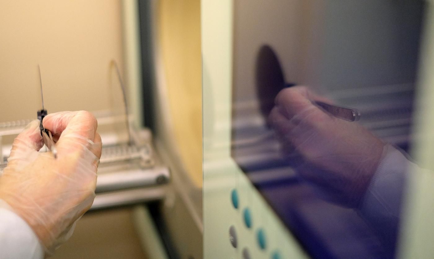
Samples surface cleanings
Cleaning of organics, particles and remaining traces of metallic (ionic) contaminants in:
- Piranha mixture, oxide stripping and RCA cleaning.
- Cleanings with solvents (acetone and isopropanol).
Wet and oxygen plasma photoresist stripping:
- Photoresist stripping in acetone.
- Photoresist stripping in acid.
- Photoresist stripping in stripper (basic mixture).
- Photoresist stripping in oxygen plasma.
Download the techniques and capabilities of the Wet Etching and Surface Cleaning Processes Area
Check the Wet Etching and Surface Cleaning Processes Area
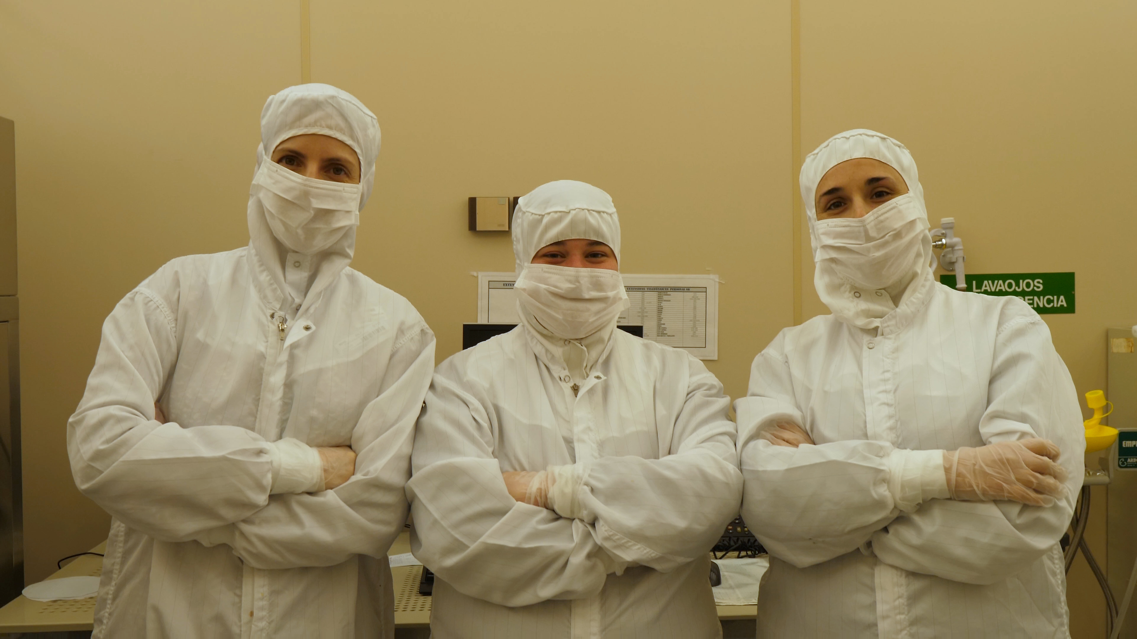
Wet Etching and Surface Cleaning Processes Team
- Nuria Torres (ext. 435568)
- Elena Chica (ext. 435580)
- Andrea Azambuja (ext. 435579)