


Equipment and processes of the Electrical Characterisation on Wafer Area
The Electrical Characterisation on wafer Area is dedicated to measuring and analyzing the electrical properties of semiconductor devices to assess their performance, uniformity, and quality in manufacturing integrated circuits.
Técnicas
- DC Measurements and Basic Parameters
- High Frequency Characterization
- Noise and Reliability Measurements
- Extreme Conditions Characterization
Equipos
Parametric test system
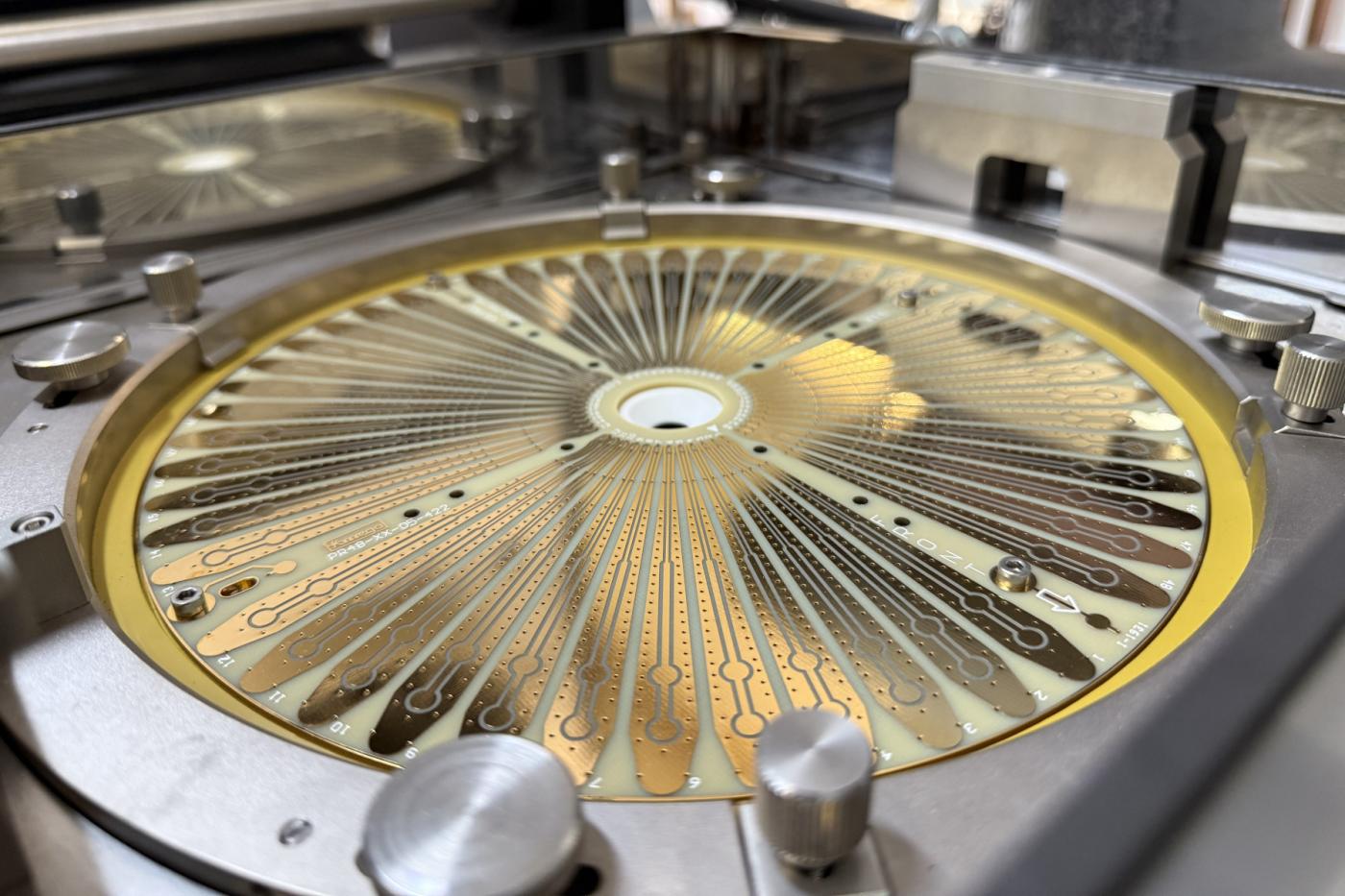
- Semi-automatic parametric test station, based on a Süss Microtech PA200 semi-automatic prober and an Agilent 41000 Parametric Test System. It has 4 SMU units, a CV meter and a switching matrix. Connection to the wafer is done through probecard.


Probers
Apart from the parametric testing system, we have 4 semi-automatic prober machines available:
- MPI TS2000-SE
- Wentworth AWP 1050 (available inside the Clean Room)
- KarlSüss PA200
- MPI TS2000-SE térmica (-40 ºC to 300 ºC)
It can be contacted on wafer or chip using micro manipulators or prober card.


General purpose on-wafer measurement equipment
These probers can be used together with the available electrical measurement equipment:
- Semiconductor parameter analysers:
- Keysight B1500
- HP4155B
- 2 Keithley 4200 (both include 4 SMU and one with CV module)
- CV measurement equipment:
- Keysight E4990
- HP4280A
- HP4192A
- small auxiliary equipment:
- Keithley 2600
- Keithley 2470


Capacidades disponibles
DC Measurements and Basic Parameters
- Source-Meter Unit (SMU - Source Measure Unit) - To measure current and voltage simultaneously.
- I-V Curves (Current-Voltage) - To characterize transistors, diodes and resistors.
- C-V Curves (Capacitance-Voltage) - To evaluate oxide quality and doping.
- Four-Point Probe - To measure thin film resistivity.
High Frequency Characterization
- Impedance and Admittance Analysis - Measurements with impedance analyzers to characterize passive devices.
- S-Parameters with VNA (Vector Network Analyzer) - To evaluate RF and microwave devices.
Noise and Reliability Measurements
- 1/f Noise Measurement (Flicker Noise) - To evaluate material quality and defects.
- Lifetime and Reliability Tests (TDDB, BTI, HCI) - To estimate degradation in MOSFET devices.
Extreme Condition Characterization
- Low Temperature Probing (down to -40ºC) - For semiconductor studies at low temperatures.
- High Temperature Measurements (Hot Chuck up to 300ºC) - To evaluate thermal behavior of devices.
Download the techniques and capabilities of the Electrical Characterisation on wafer Area
Electrical Characterisation on wafer Team
- Sergi Sánchez (ext. 435558)
- Mónica Sarrión (ext. 435581)