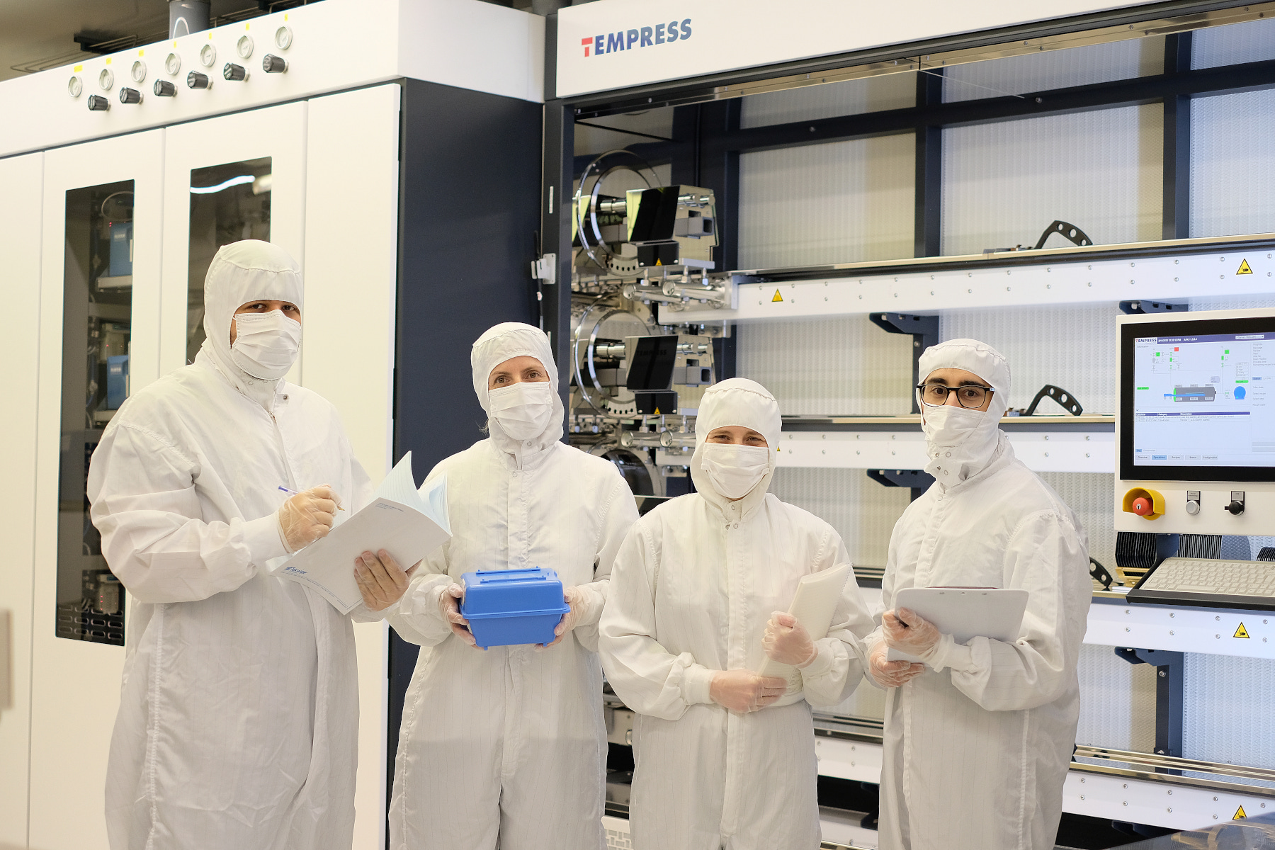
Equipment and processes of the Thermal Processes Area
The Thermal Processes Area is a main space where critical techniques in micro and nanofabrication are performed, such as Thermal silicon oxidation, Low pressure chemical vapor deposition (LPCVD) or Plasma-enhanced chemical vapor deposition (PECVD).
Techniques
- Thermal silicon oxidation
- Diffusion and annealing processes
- Rapid thermal processing (RTP)
- Low pressure chemical vapor deposition (LPCVD)
- Plasma-enhanced chemical vapor deposition (PECVD)
- Atomic layer deposition (ALD, PEALD)
Equipment
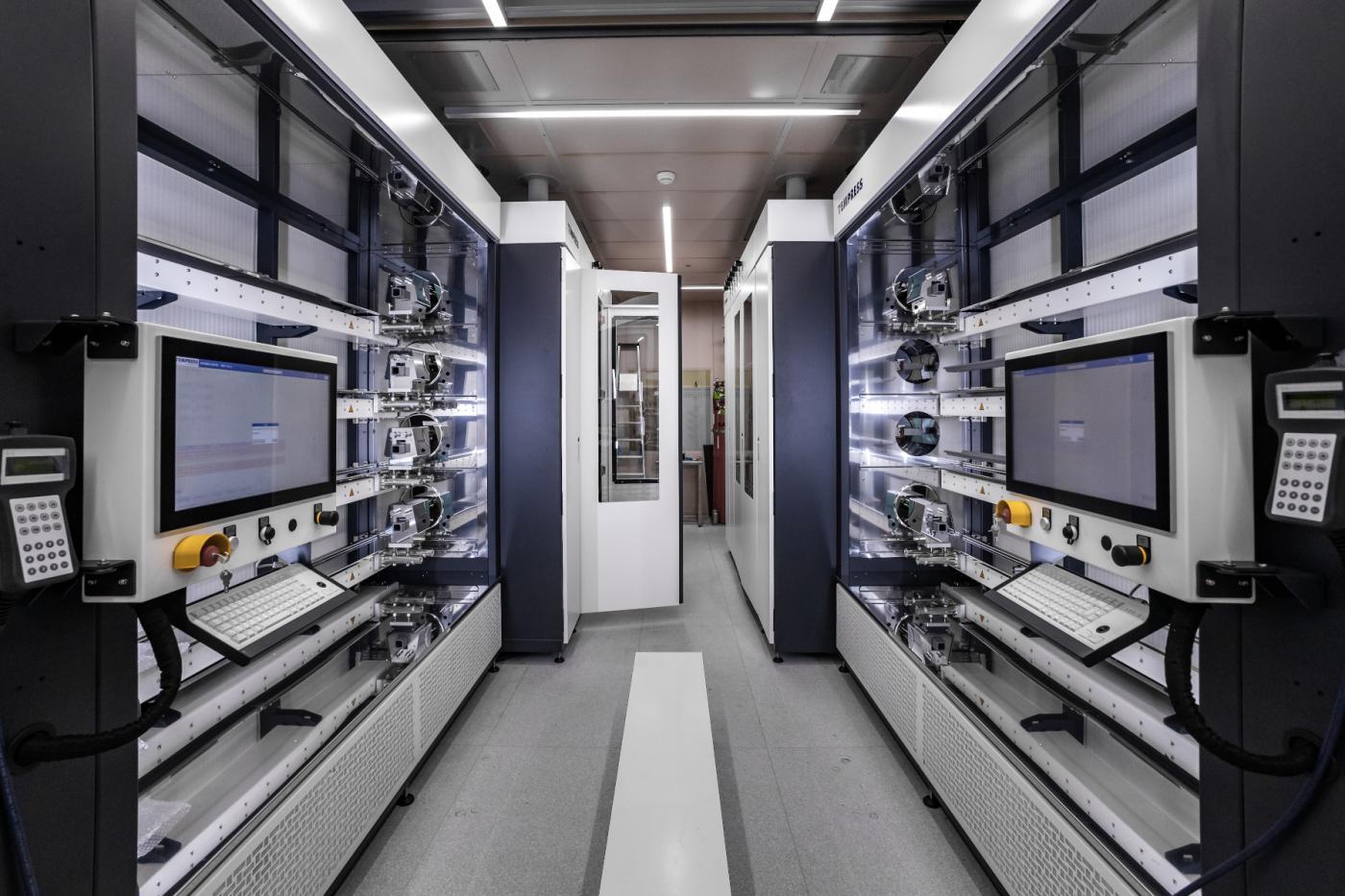
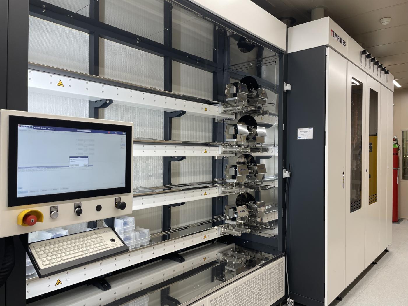
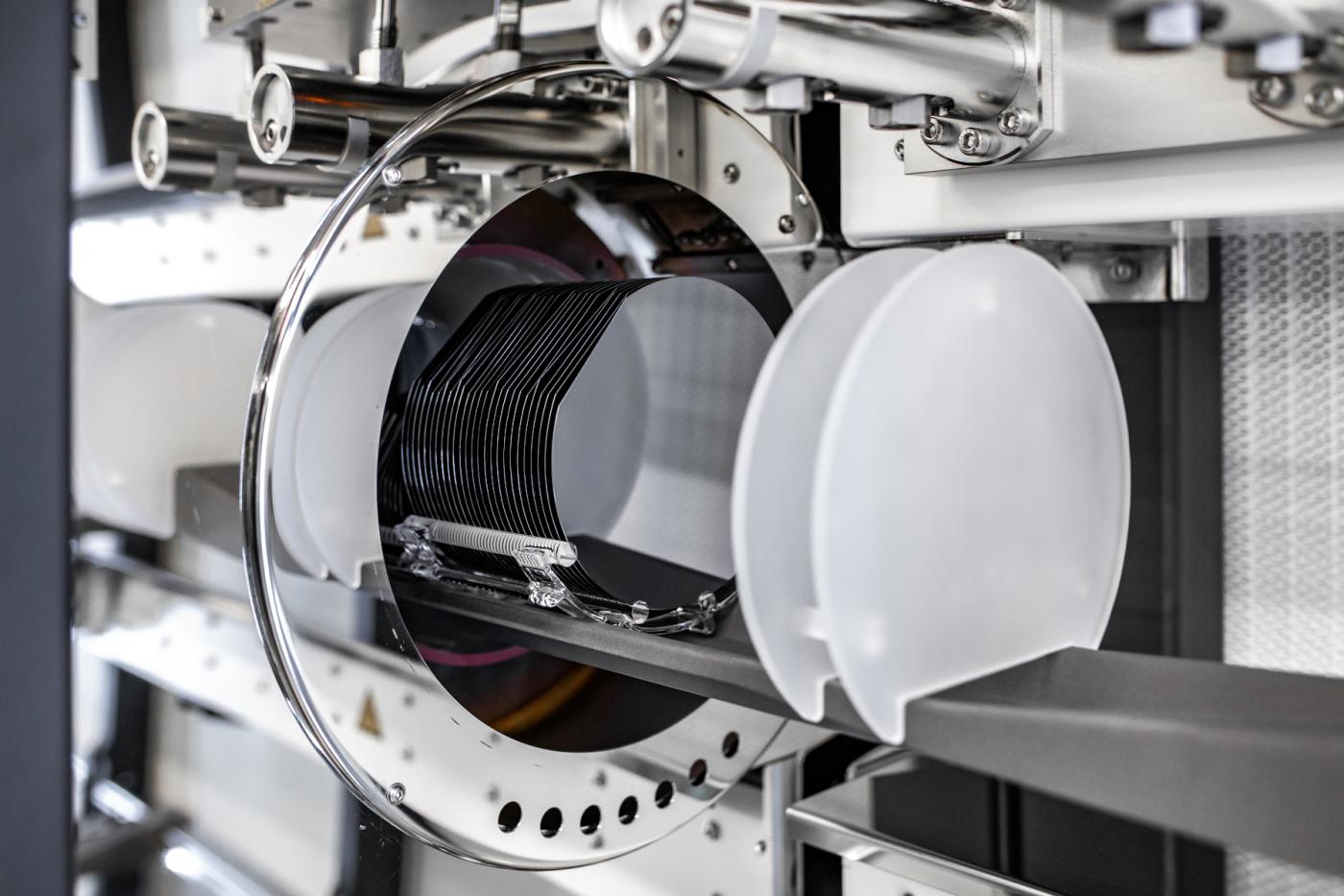
Thermal silicon oxidation, diffusion and annealing processes and low-pressure chemical vapor deposition (LPCVD)
4 racks of 4 horizontal tubular furnaces each. 15 furnaces are allowed to process CMOS (clean) samples, and 1 is dedicated to MNC processing (metal contaminated samples). Wafers up to 150 mm diameter or below.
- Brand: Tempress, Model: TS-Series V
- Furnace: AFS
- Brand: Tempress, Model: TS-Series V
- Furnace: AFT
- Brand: Tempress, Model: TS-Series V
- Furnace: AFU
- Brand: Tempress, Model: TS-Series V
- Furnace: AFK
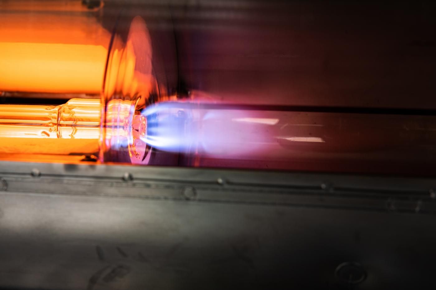
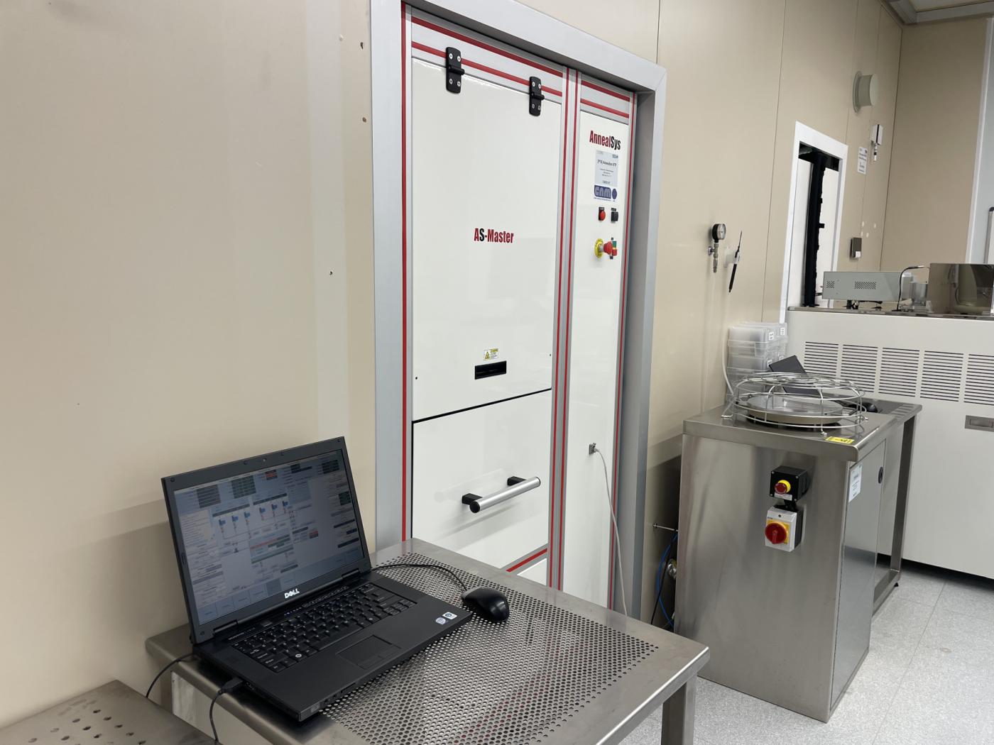
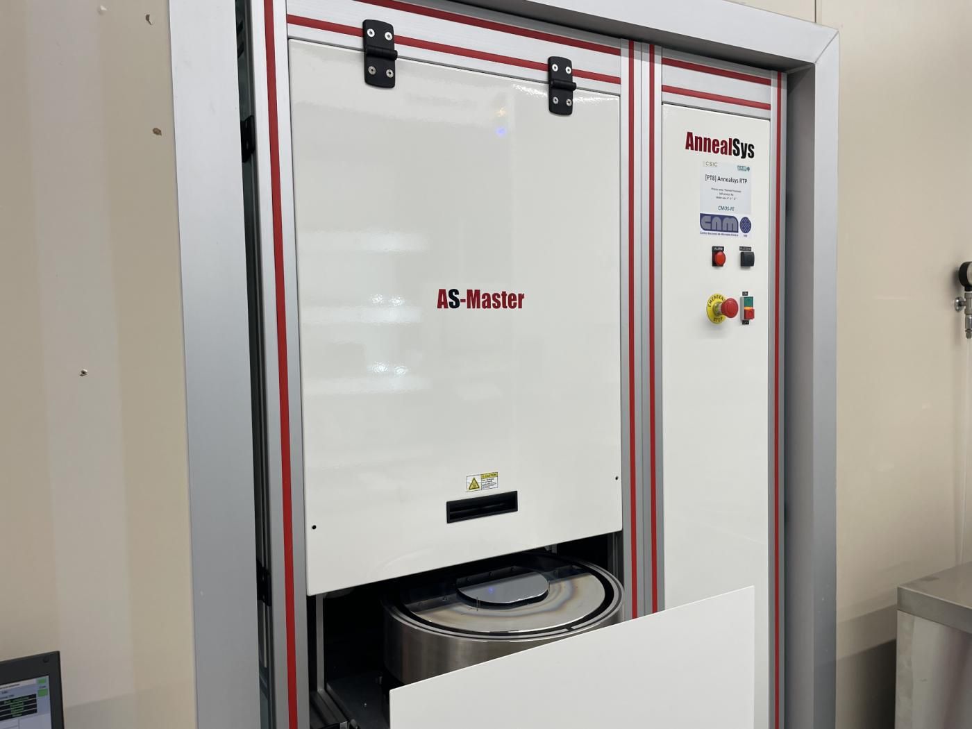
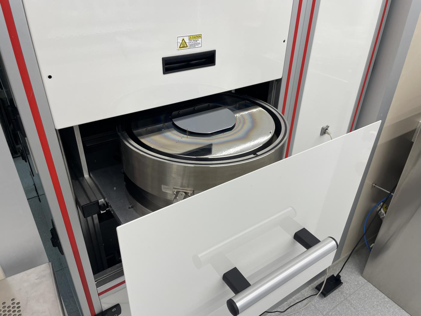
Rapid thermal processing (RTP)
- Annealsys, AS-Master-2000: 1 chamber. CMOS processing (clean samples). Wafers up to 200 mm diameter or below.
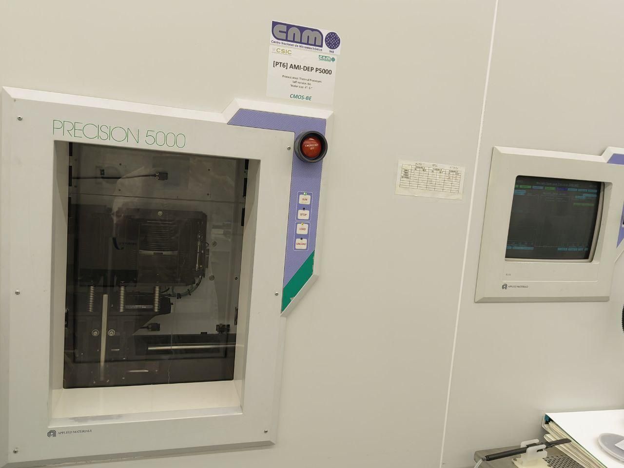
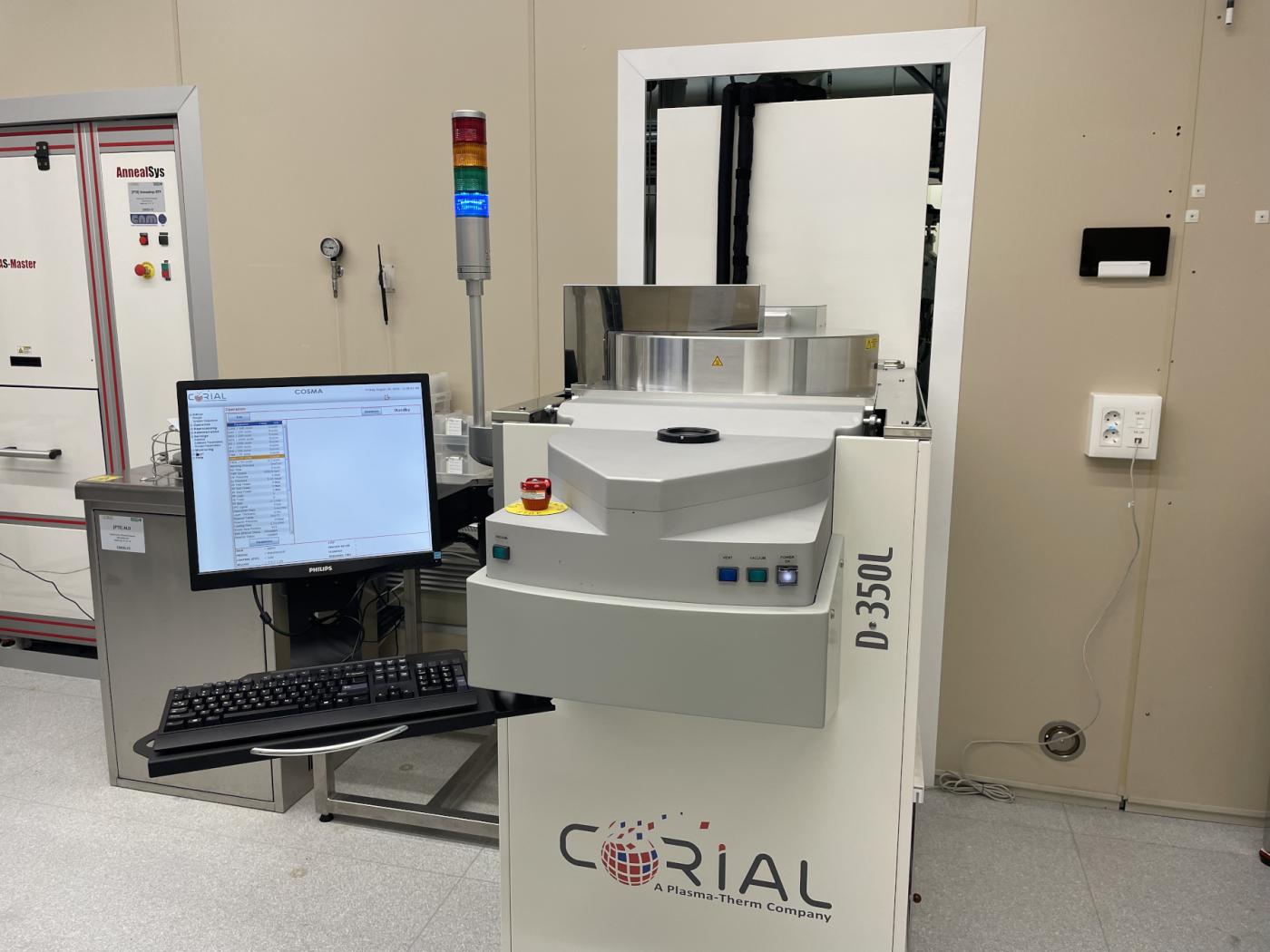
Plasma-enhanced chemical vapor deposition (PECVD)
- Applied Materials, Precision 5000 Mark II: 1 tool with 3 chambers. CMOS processing (clean samples). Wafers up to 150 mm diameter.
- Corial, D350L: 1 chamber. CMOS (clean samples). Wafers up to 150 mm diameter.
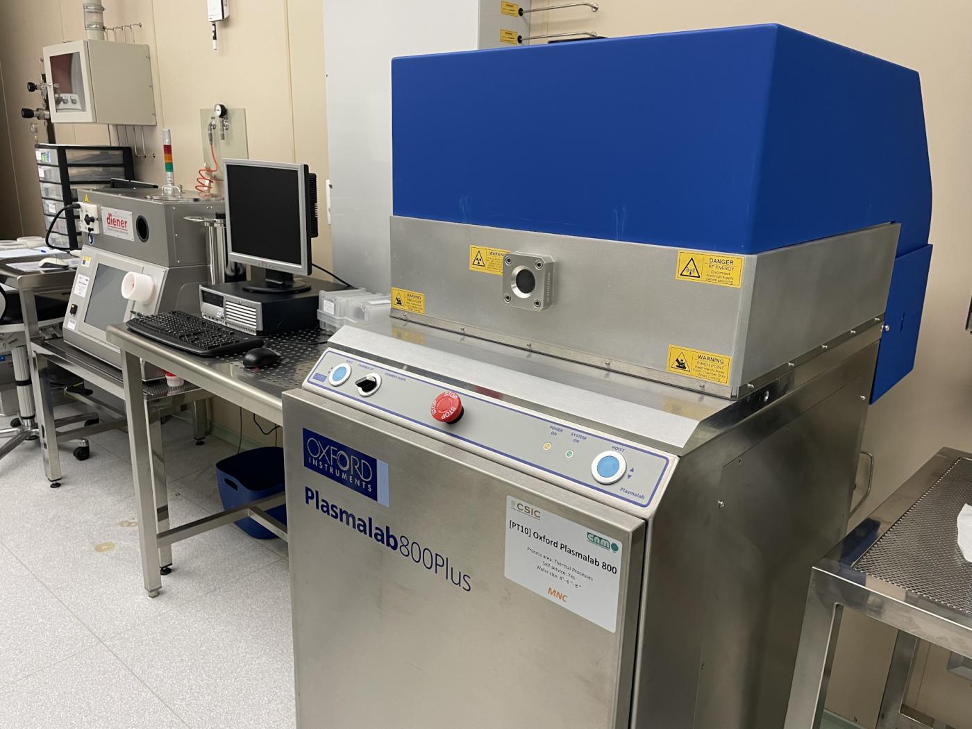
- Oxford IPT, Plasmalab 800 Plus: 1 chamber. MNC processing (metal contaminated samples). Wafers up to 200 mm diameter
Atomic layer deposition (ALD, PEALD)
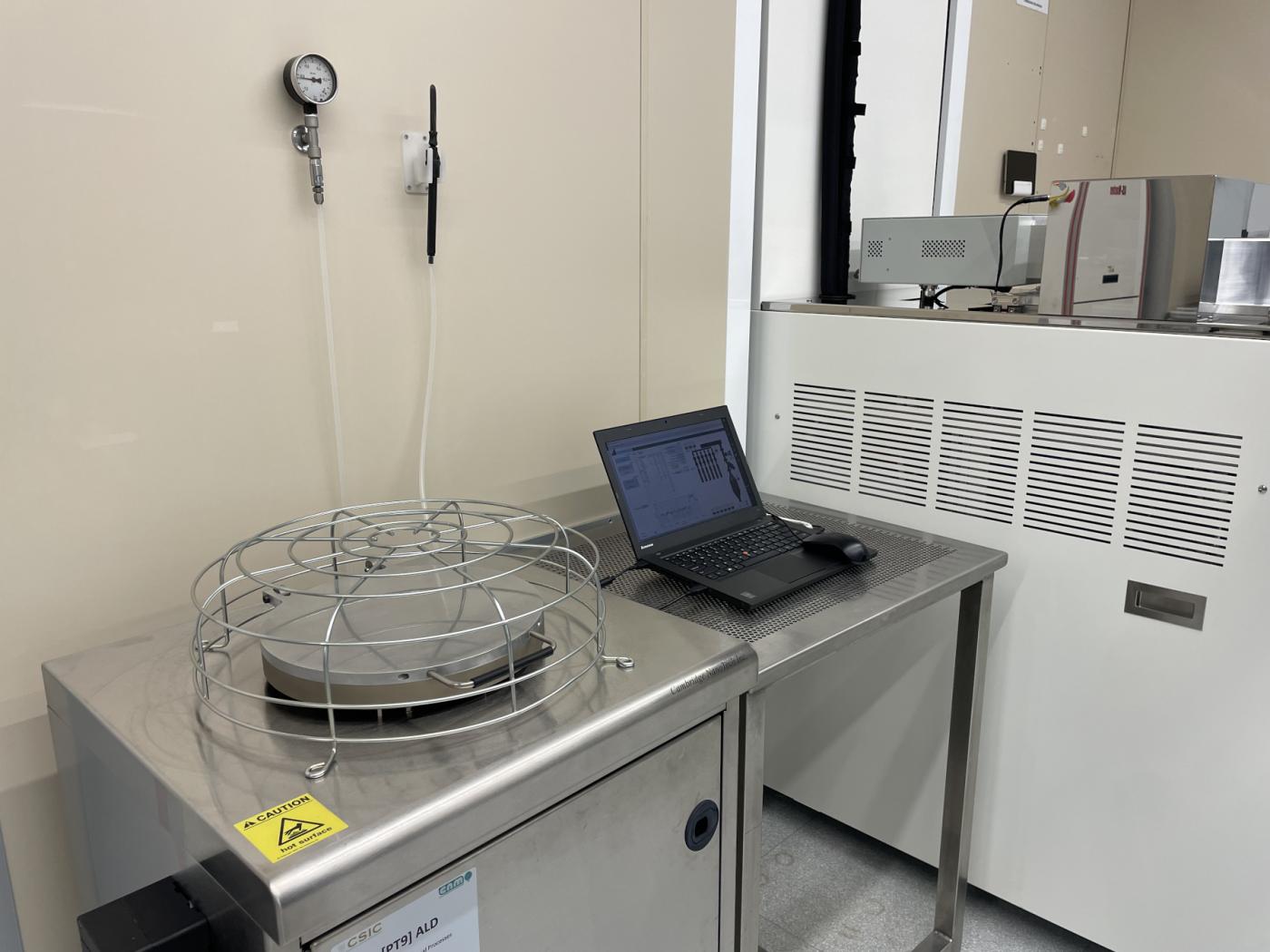
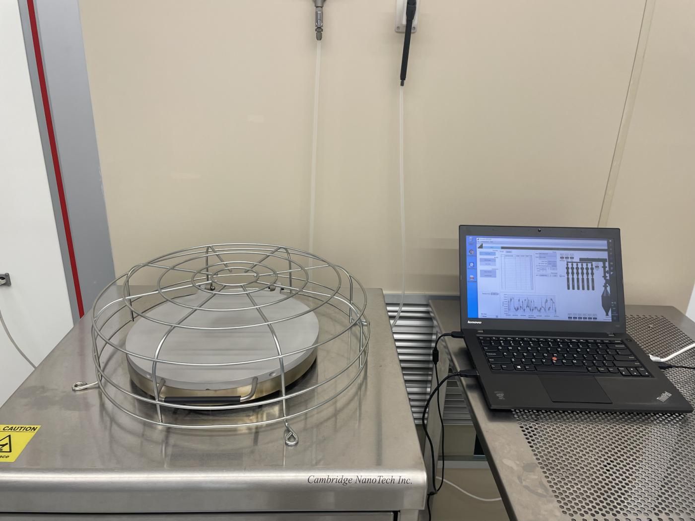
- Thermal: Cambridge Nanotech, Savannah 200: 1 chamber. CMOS processing (clean samples). Wafers up to 200 mm diameter.
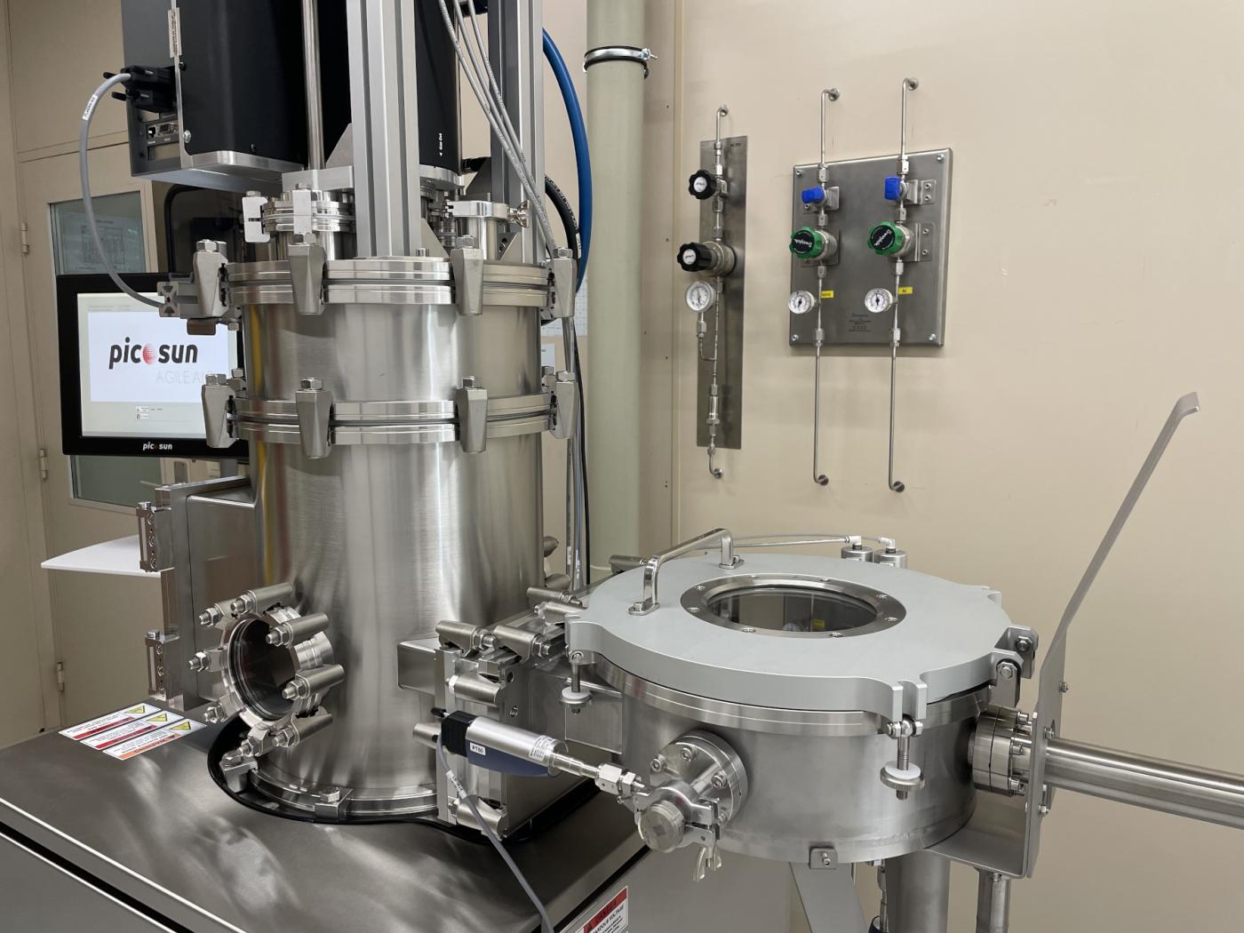
- Thermal and plasma enhanced: Picosun, R200 Advanced: 1 chamber. MNC processing (metal contaminated samples). Wafers up to 200 mm diameter.

Available capabilities
Thermal silicon oxidation
- Temperature range from 900ºC to 1100ºC
- H2 & O2 or H2O with C2H2Cl2 environment
- Thickness range from 5 nm up to 3000 nm
- In-wafer and wafer to wafer uniformity below 1%
- Batch capacity 50 wafers
Diffusion and annealing processes
- Annealing in N2, O2, N2O or Ar environment from 600ºC to 1300ºC
- Aluminum annealing in N2/H2 environment from 250ºC to 450ºC
- MNC thermal annealing from 600ºC to 1100ºC
- Phosphorus pre-deposition (Liquid source, POCl3)
- Boron pre-deposition (Liquid source, BBr3)
- Batch capacity 50 wafers
Rapid thermal processing (RTP)
- Rapid thermal annealing (RTA) available under O2, N2, N2O and Ar environment from 400ºC to 1200ºC
- Rapid thermal oxidation (RTO) available under O2 environment from 400ºC to 1200ºC
- Single wafer system
Low pressure chemical vapor deposition (LPCVD)
- Silicon nitride (Si3N4) deposition at 800ºC for thicknesses from 10 nm to 300 nm
- Low stress silicon nitride (Si3N4) deposition at 850ºC for thicknesses from 10 nm to 300 nm
- Polysilicon (PolySi) deposition at 630ºC for thicknesses from 30 nm to 3 μm
- Amorphous silicon (a-Si) at 565ºC for thicknesses from 30 nm to 3 μm
- Silicon oxide (SiO2) at 700ºC for thicknesses from 50 nm to 300 nm
- In-wafer and wafer to wafer uniformity below 3%
- High quality films and good step coverage
- Batch capacity 25 wafers
Plasma-enhanced chemical vapor deposition (PECVD)
Applied Materials – Precision 5000 mark II
- Automatic single wafer multi-chamber system with cassette
- Silicon oxide (SiO2) deposition at 400ºC for thicknesses from 50 nm to 5 μm
- Two silicon precursors available: Tetraethyl orthosilicate (TEOS) and Silane (SiH4)
- Silicon nitride (Si3N4) deposition at 400ºC for thicknesses from to 50 nm to 1 μm
- Passivation layer: Silicon oxide (SiO2) combined with Silicon nitride (Si3N4) at 375ºC as diffusion barrier and against-moisture layer
- In-wafer and wafer to wafer uniformity below 10%
- Batch capacity 15 wafers
Corial – D350L
- Silicon oxide (SiO2) deposition up to 320ºC for thicknesses from 50 nm to 5 μm
- Two silicon precursors available: Tetraethyl orthosilicate (TEOS) and Silane (SiH4)
- Silicon nitride (Si3N4) deposition up to 320ºC for thicknesses from to 50 nm to 1 μm
- Amorphous silicon deposition (a-Si:H) at 200ºC for thicknesses from 50 nm to 500 nm
- Deposition of doped silicon oxide (with Boron and/or Phosphorous) at 320ºC to form BSG (borosilicate glass), PSG (phosphosilicate glass) or BPSG (borophosphosilicate glass) for planarization capabilities, and thicknesses between 1 μm – 2 μm
- In-wafer and wafer to wafer uniformity below 10%
- Batch capacity of 7 wafers of 100 mm or 1 wafer of 150 mm
Oxford IPT - Plasmalab 800 Plus
- Silicon oxide (SiO2) deposition (SiH4) at temperatures up to 380ºC for thicknesses from 50 nm to 5 μm
- Silicon nitride (Si3N4) deposition at temperatures up to 380ºC for thicknesses from 50 nm to 1 μm
- Amorphous silicon (a-Si:H) deposition up to 300ºC for thicknesses from 50 nm to 1 μm
- Dual frequency plasma available (13.56 MHz/350 kHz) for low stress silicon oxide and silicon nitride layers
- In-wafer and wafer to wafer uniformity between 10%
- Batch capacity of 8 wafers of 100 mm, 4 wafers of 150 mm or 1 wafer of 200 mm
Atomic layer deposition (ALD)
Cambridge Nanotech - Savannah 200
- Temperature range: from 150ºC to 350ºC
- Thicknesses from 0.5 nm to 50 nm
- Aluminum oxide (Al2O3)
- Hafnium oxide (HfO2)
- Titanium oxide (TiO2)
- Nanolaminates
- 2 types of oxidant precursors: D. I. H2O and O3
- In-wafer thickness uniformity around 1-2%
- Batch capacity of 2 wafers of 100 mm, 1 wafer of 150 mm or 1 wafer of 200 mm
Picosun - R200 Advanced
- Temperature range: from 60ºC to 300ºC
- Thicknesses from 0.5 nm to 50 nm
- Aluminum oxide (Al2O3), thermal and plasma enhanced
- Hafnium oxide (HfO2), thermal and plasma enhanced
- Titanium oxide (TiO2), thermal
- Silicon oxide (SiO2), plasma enhanced
- Nanolaminates
- Sequential infiltration synthesis (SIS)
- 2 types of oxidant precursors: D. I. H2O and P. E. O2
- In-wafer thickness uniformity around 1-2%
- Single wafer system
Download the tecniques and capabilities of the Thermal Processes Area
Thermal Processes Team
- Sara Durán (ext. 435561)
- Ricard Noy (ext. 435554)
- Elena Chica (ext. 435580)
- Olaf Vázquez (ext. 435688)