Equipment and processes of the Ion Implantation Area
The Ion Implantation Area is the area where the wafer surface doping technique is performed. Depending on the equipment used, the following atomic species can be implanted: B, P, As, N, Ar, Al, Si, Mg, O, He.
Techniques
- Precise control on doping depth profile.
- Low temperature process, i. e. compatible with photoresist mask.
- Wide selection of masking materials: photoresist, oxide, poly-Si, metal…
- Lateral doping uniformity.
Equipos
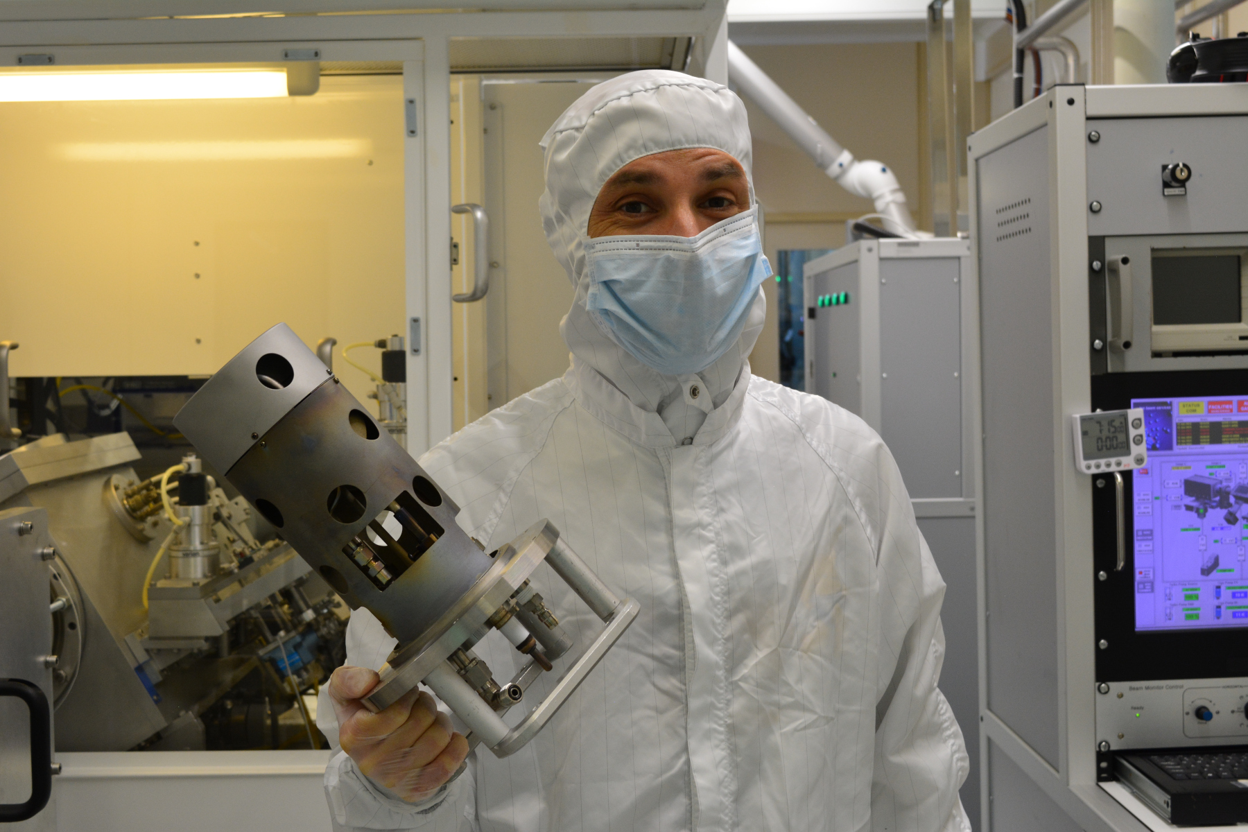
Ion Implanter IBS IMC 210RD:
- Liquid, gas and solid sources.
- Available precursors: BF3, SiF4, N2, Ar, CO2, He/Ar, As, P, Mg, AlCl3, GeS2 and H2O.
- Implanted doses from 1.0×10¹¹ at/cm2 to 5.0×10¹⁵ at/cm2.
- Energy range: from 3 keV to 210 keV (single charge).
- Equipped with two processing chambers: standard (ES) and research and development (RD) chambers.
- ES chamber: Automated loading system.
- RD chamber: Manual loading system. Possibility to process thin wafer (thickness<400 µm) and small pieces. Holder allows to heat wafers up to 500ºC.
- Tilt range: From 0° to 15° and from 0° to 10° at ES chamber and RD chamber, respectively.
- Maximum wafer size: 4 inch wafers and 6 inch wafers for ES and RD chamber, respectively.
- Temperature: Possibility to heat wafer up to 500 °C.
- Exclusively to process CMOS samples.


Download the techniques and capabilities of the Ion Implantation Area
Ion Implantation Team
- Alberto García (ext. 435556)
- Aniol Vellvehí (ext. 435551)