Equipment and processes of the Packaging Area
The Packaging area is the area in the Clean Room where tasks such as wafer dicing, die bonding or flip-chip are performed
Techniques
- Silicon wafers and different materials substrates dicing and cleaving
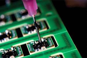
- Microelectronic devices Packaging: dispensing epoxy adhesives, wirebonding, ribbon bonding, Flip Chip, etc.
- Circuit Packaging test: destructive or non destructive test, wire bond shear test, die attach test by shear test, etc.
Equipment and Available capabilities
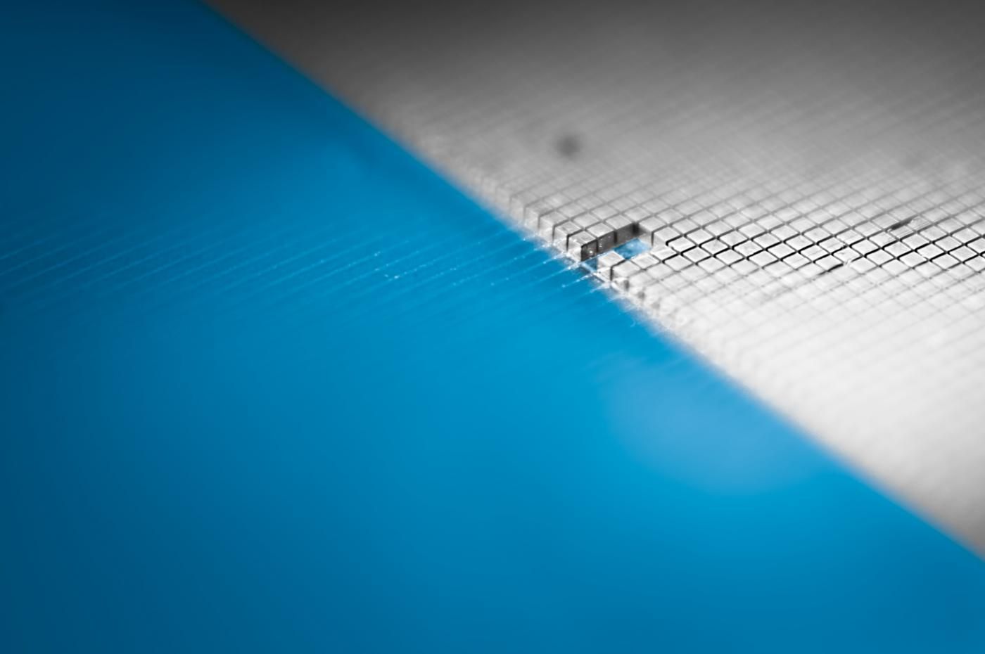
Substrate dicing
Semiautomatic Dicing machine K&S780
- Semi-automatic equipment
- Substrates up to 6”
- Y-axis accuracy: 2 µm
- Hub and hub less type 2" blades
- Multiple chip dimensions
- Multiple cutting depths
- Multiple rotation angles: Parametric
- Sawable substrate materials: Si, Ge, GaAs, GaN, Borosilicate, Al2O3, SiO2, SiC, LiNbO3
Dicing Machine K&S 980 (1998)
- Semi-automatic equipment
- Substrates up to 8"
- Y-axis accuracy: 2 µm
- Hub and hub less type 2" blades
- Multiple chip dimensions
- Multiple cutting depths
- Multiple rotation angles: By reference
- Sawable substrate materials: Si, Ge, GaAs, GaN, Borosilicate, Al2O3, SiO2, SiC, LiNbO3

Dicing Machine DISCO DAD-3350 (2019)
- Substrates up to 8"
- Circle cut for wafer downsizing
- US option for SiC
- In process checking
- CO2 Bubbler
- Additives for long-term processes
- Highly configurable and programmable with wizards and PRS
- Higher dicing quality with lower environmental impact
- Sawable substrate materials: Si, Ge, GaAs, GaN, Borosilicate, Al2O3, SiO2, SiC, LiNbO3
LatticeGear 420 Cleaver (2015)
- Cleaves almost all crystalline materials
- Clock dial for indent calibration
- Indent position control with 5 µm step size
- High accuracy positioning of sample (±10 µm)
- Resulting sample size down to 5 mm
- Polished tip diamond indenter with polished face for accurate positioning
- Colour CCD camera and Monocular, parfocal, zoom lens
- Up to 300 mm substrate size
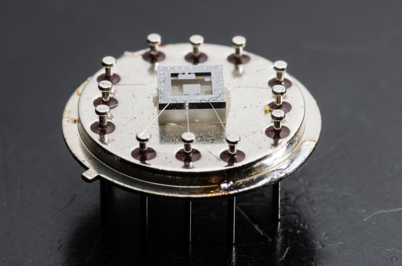
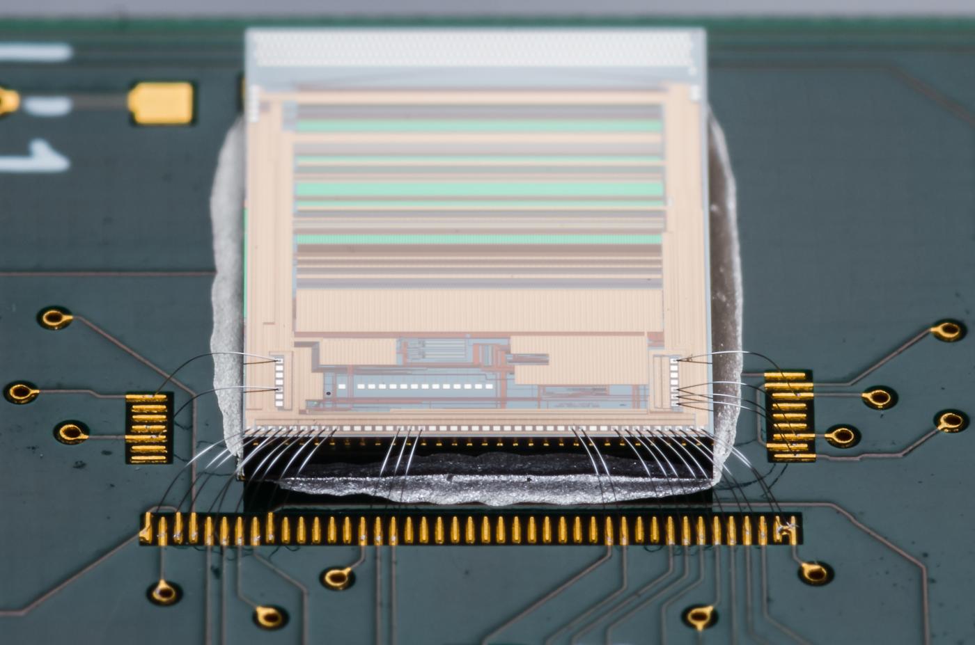

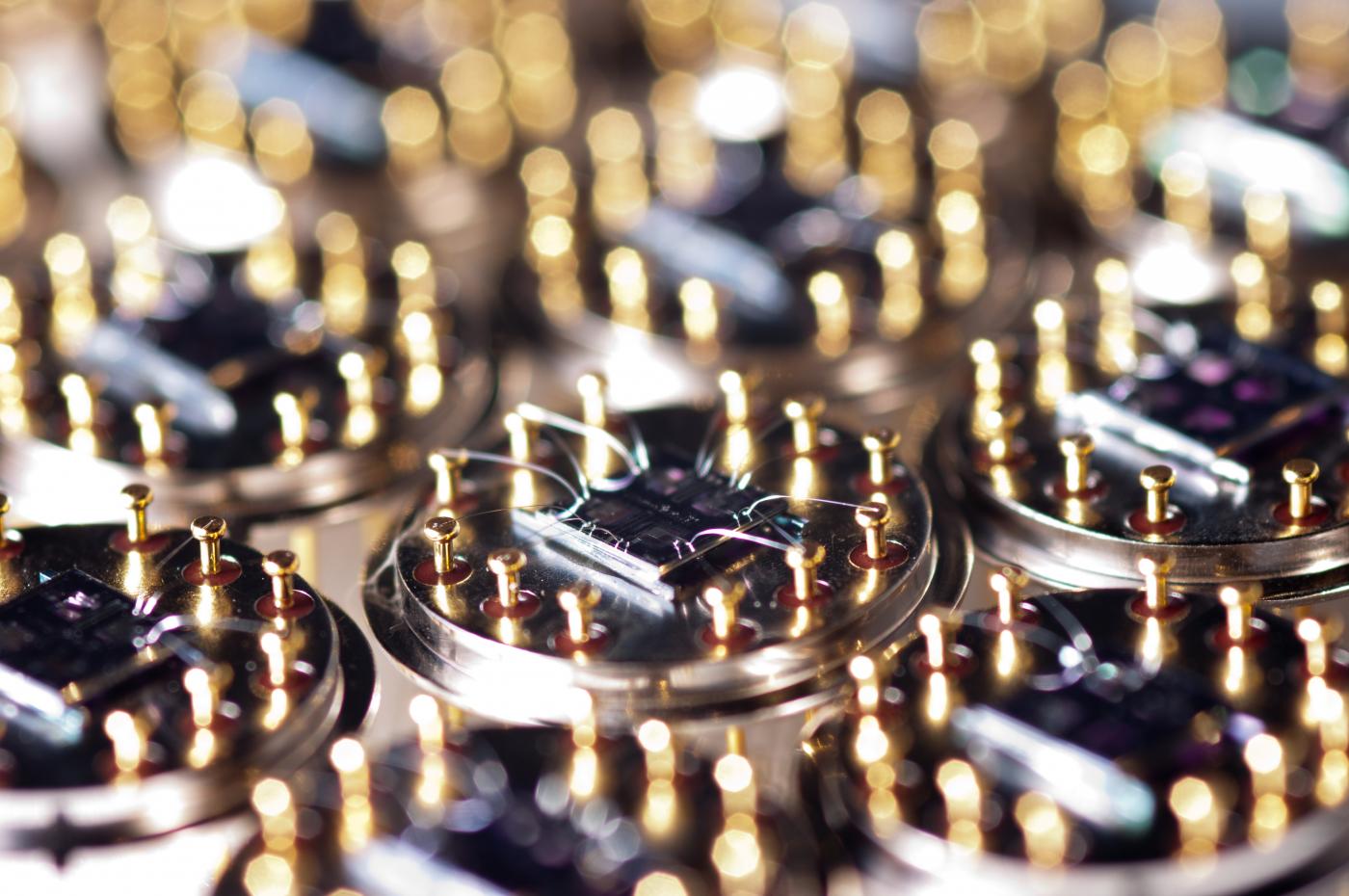
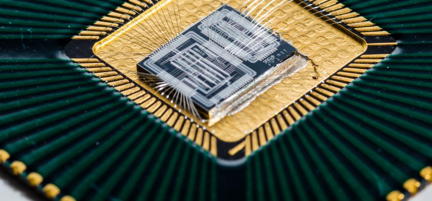
Microelectronic devices Packaging
Dr. Tresky T4907 (2006)
- Manual Pick&Place
- Epoxy and soft paste dispenser
- Rework Station
- Flip chip option installed
- Placement accuracy: 10 µm
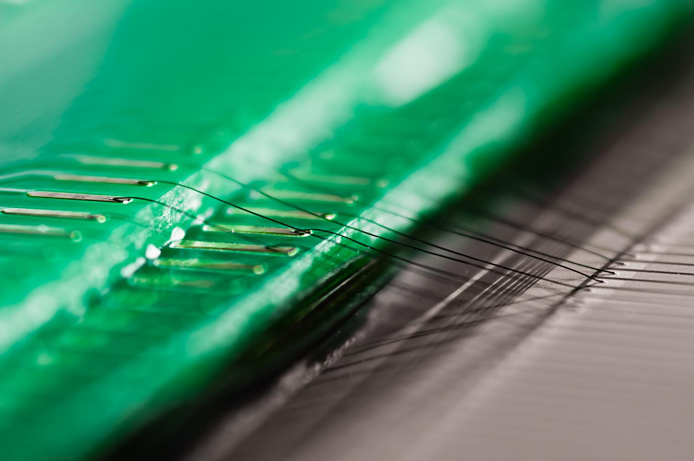
K&S 4123, 4523, 4127 Wedge Bonders (1986 y 2005)
- Fully manual bonders
- Accepts standard packages and substrates up to 4"
- Al, Au and Cu wires from 0.7 to 15 mils
- Heated sample holder
- Target light beam system
Wire Bonder TPT HB16 (2009)
- Semi auto, Deep Access wire and Ribbon Bonder
- Au, Al, Ag, Cu wire (17 to 75 µm) for Wedge & Ball Bonding
- Au and Al Ribbon up to 250 x 25 µm
- Large program storage capacity with more than 100 parameters
- Accepts flat packages and substrates up to 4"
- Heated sample holder
- Spotlight targeting system
- Possibility to make bumps for Flip-chip packaging


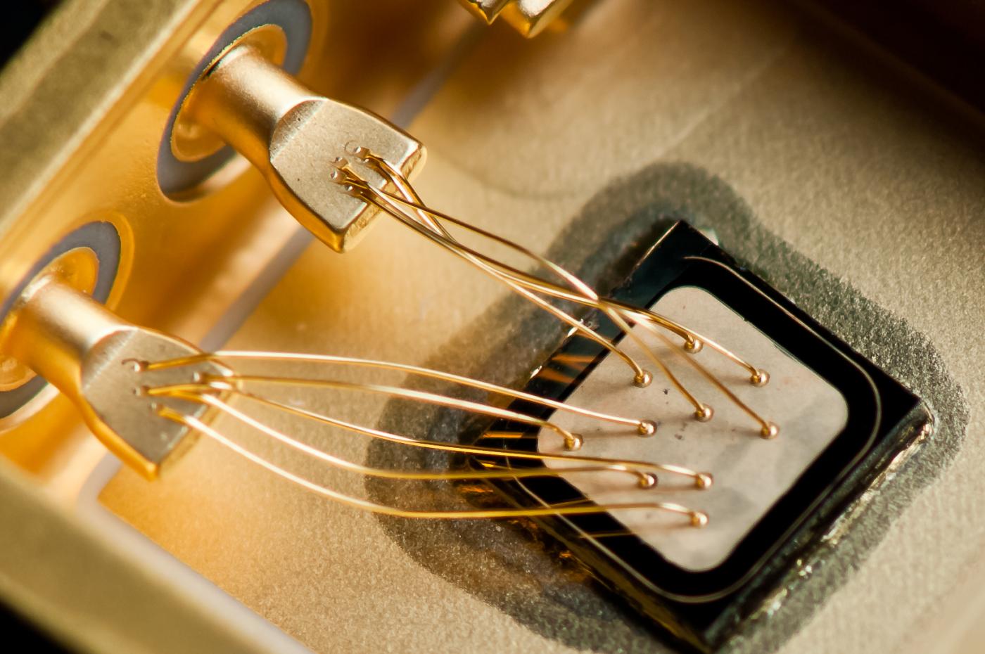
Bondtec 56XXi Wirebonder & Bond Tester (2022)
- Changeable bondheads for all wirebond and testing process
- Installed ball bonding (5610i) and Deep access wire bonding heads (5632i)
- Installed Pullheads - 100 cN - 5000 cN and Shearheads - 500 cN - 5000 cN
- Automatic bonding with pattern recognition system
- Adaptable bond settings (loop shapes, force and power profiles…), stored in unlimited bond programs
- Travel distances 100 mm x 100 mm
- Up to 1800 bonds/h
Royce 650 Die Shear & Bond Tester (2010)
- 305 mm x 155 mm stage for 300 mm wafers, leadframes or substrates
- Interchangeable test heads
- Die shear up to 200 kgf
- Wire Pull Test Force up to 10 kgf
- Total System Accuracy: ±0.1 %


Download the tecniques and capabilities of the Packaging Area
Packaging Team
- Alberto Moreno Garriga (ext. 435572)
- María Sánchez Martínez (ext. 435573)