Equipment and processes of the Inspection and Measurement Area
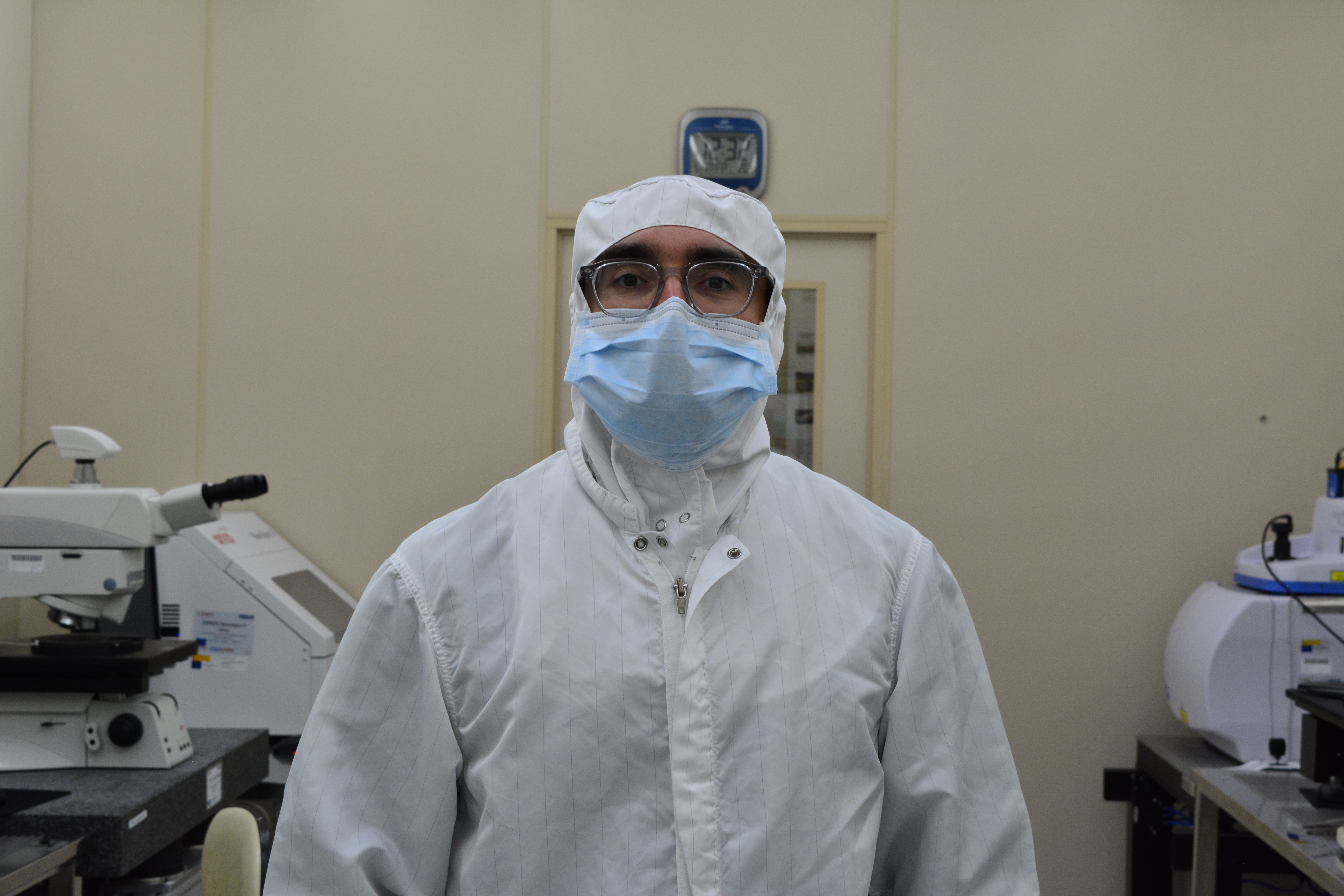
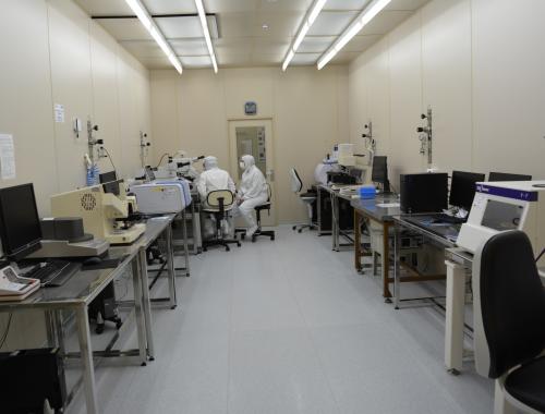
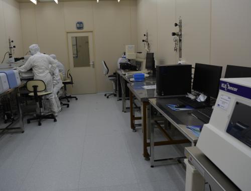
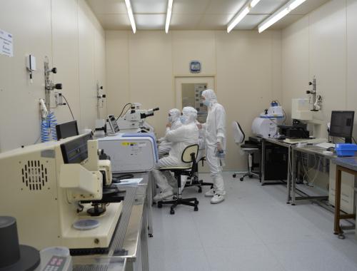
The Inspection and Measurement Area is the area in charge of two specific tasks: to verify that, after each process, the wafers are free of particles and defects and to characterize the deposited or etched layers by measuring different parameters (optical, electrical, mechanical, etc).
Techniques
- Optical Microscopy
- Spectral Reflectance
- Spectral Ellipsometry
- 3D optical Profilometry
- Mechanical Profilometry
- FT-IR Spectroscopy
- Sheet Resistance measurement
- Bow and Thickness measurement
- Life Time measurement
Equipment
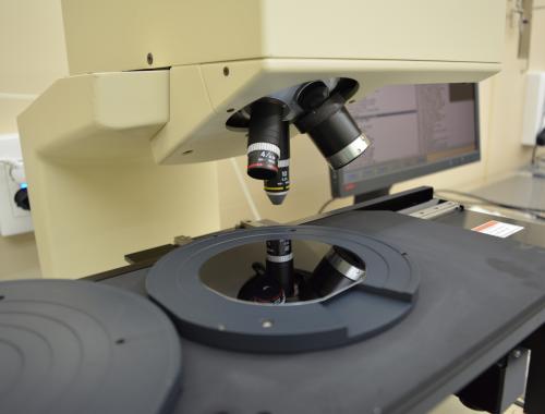
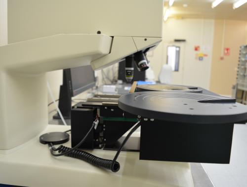
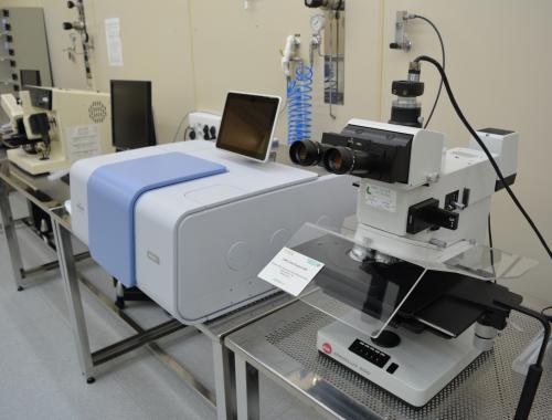
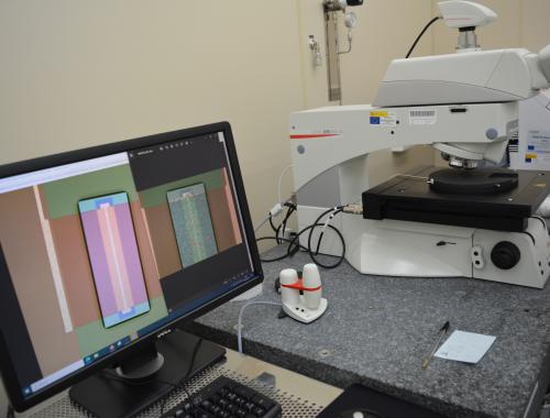
Optical Microscope: Leica DM8000
- Surface analysis: Defects and Particles
- Dimensions measurements
- Wafer-mapping
- Photomicrography
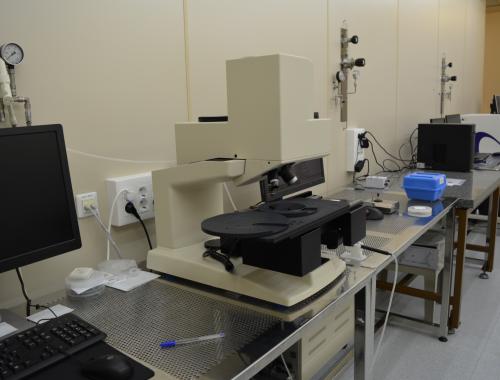
Spectral reflectometers: Nanospec 6100 and Nanospec II
- Thickness measurement of transparent layers
- Spectral Range: 440-1000 nm
- Predeterminated materials library
- New material analysis
- Multiple layer analysis
- Automatic XYZ stage
- Wafer mapping
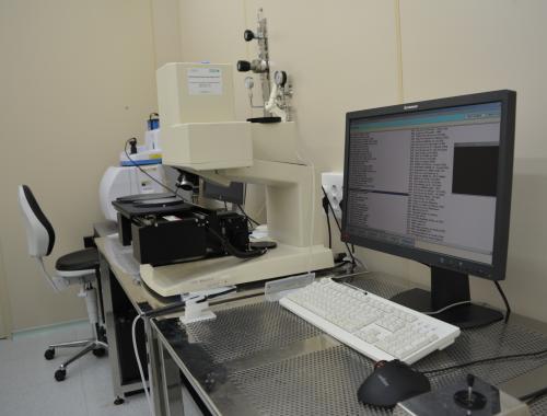
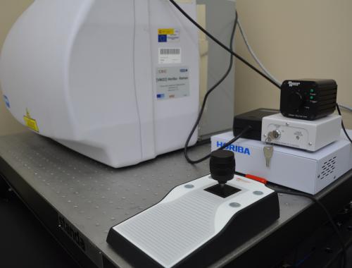
Spectral Ellipsometer: Horiba Auto SE
- Full analysis of thin films: thicknesses, optical constants, surface roughness, etc
- Automatic XYZ stage
- Real-time imaging
- Automatic selection of spot size
- Spectral range: 440-1000 nm
3D optical profilometer: Sensofar Neox
- Extract topographical data: surface morphology, step heights and surface roughness
- Fast data acquisition over large areas
- Noncontact and non-destructive measurements
- Large Z-axis range, feature heights from few nanometers up to 2cm
- Variable field of view
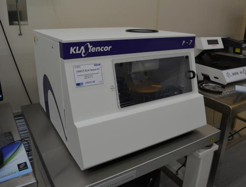
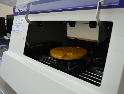
Mechanical Profilometers: Tencor P7 (x2, CMOS and MNC lines)
- Profile and roughness measurement in any type of sample (Transparent or Opaque)
- High accuracy in horizontal measurements: 1 um displacements
- Wide range in vertical measurements: 1 Å - 180 um
- Non-destructive technique for metals and semiconductors measurements
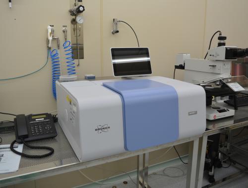
FT-IR Spectrometer: Bruker Invenio-S
- Qualitative and quantitative chemical analysis of layers (Si-O, Si-N…), dopants (P-O, B-O…) and impurities (NH, Si-H…).
- Spectral resolution: 8000-340 cm-1.
- Spectral resolution better than 0,4 cm-1
Four point probe Resistivity Measurement: Chang Min Four (x2, CMOS and MNC lines)
- Resistivity measurement of thin layers of conductive and semiconductor materials
- Characterization of uniformity in the metal deposit, polysilicon doping and ion implantation
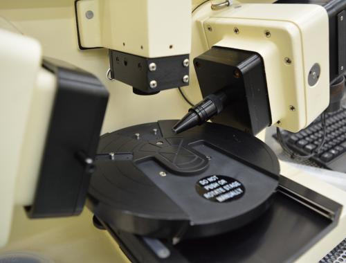
Geometrical characterization: Proforma 300
- Bow and Total Thickness capacitive measurement
- One-point non-contact
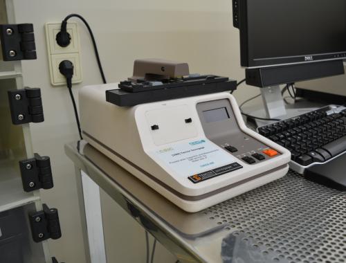
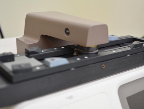
Tencor Sonogage RT2
- Resistivity and wafer Thickness measurement
- Wafer thickness measurement
- Bulk resistivity characterization
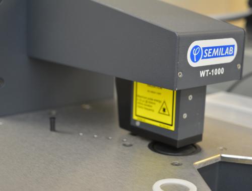
Carrier lifetime Measurement: Semilab WT-1000
- Incoming wafer characterization
- Measurement of electrical parameters in different manufacturing steps
- Characterization of deposited layer parameters
Available capabilities
- Surface and particle analysis.
- Thickness measurement of transparent layers using optical techniques: SiO2, Si3N4, Al2O3, PolySi, HfO2, etc.
- Analysis of the optical characteristics of materials.
- Mechanical profilometry of surfaces and study of the roughness of substrates and deposited layers.
- FT-IR spectroscopy of materials deposited on wafers.
- Measurement of the resistivity of substrates, metals and doped semiconductors.
- Wafer thickness and curvature measurement.
- Lifetime measurement of minority carriers.
Download the techniques and capabilities of the Inspection and Measurement Area
Check the Inspection and Measurement Area
Inspection and Measurement Team
- Samuel Dacunha Pazos (ext. 435571)
