


Educational contents on microelectronics
Educational and audiovisual materials produced by IMB-CNM to support activities on micro and nanoelectronics and to illustrate scientific concepts in educational centers, workshops and other events.
One of the objectives of the IMB-CNM's Scientific Culture strategy is to bring research activity and science closer to society, more specifically, everything related to the functioning of the electronics that surrounds us, the manufacture and the design of microelectronic circuits. Due to the public nature of the research center, the goal is to promote and favor a society with scientific curiosity, that bets on knowledge and scientific rigor, as well as aware of the value of investing in research. In addition, promoting scientific literacy among young people is one of the most effective ways to awaken interest and vocations in the field of STEAM (Science, Technology, Engineering, Art and Mathematics).
The materials on this page have been designed by the team that integrates the outreach activities of the IMB-CNM and are a support to illustrate microelectronic concepts and to learn about the operation of a research center, as well as the activity of the IMB-CNM itself.
The Scientific Culture team of the institute makes available to interested people some didactic materials developed for workshops, guided tours and talks for teachers or education professionals who wish to use them. All these works are licensed under a Creative Commons Attribution-NonCommercial-NoDerivs 4.0 International ( CC BY-NC-ND 4.0 Deed ) license.

This work is licensed under a Creative Commons Attribution-NonCommercial-NoDerivs 4.0 International.
For more information about its use, doubts or questions, the contact email address is: cultura@imb-cnm.csic.es.
Game of Transistors
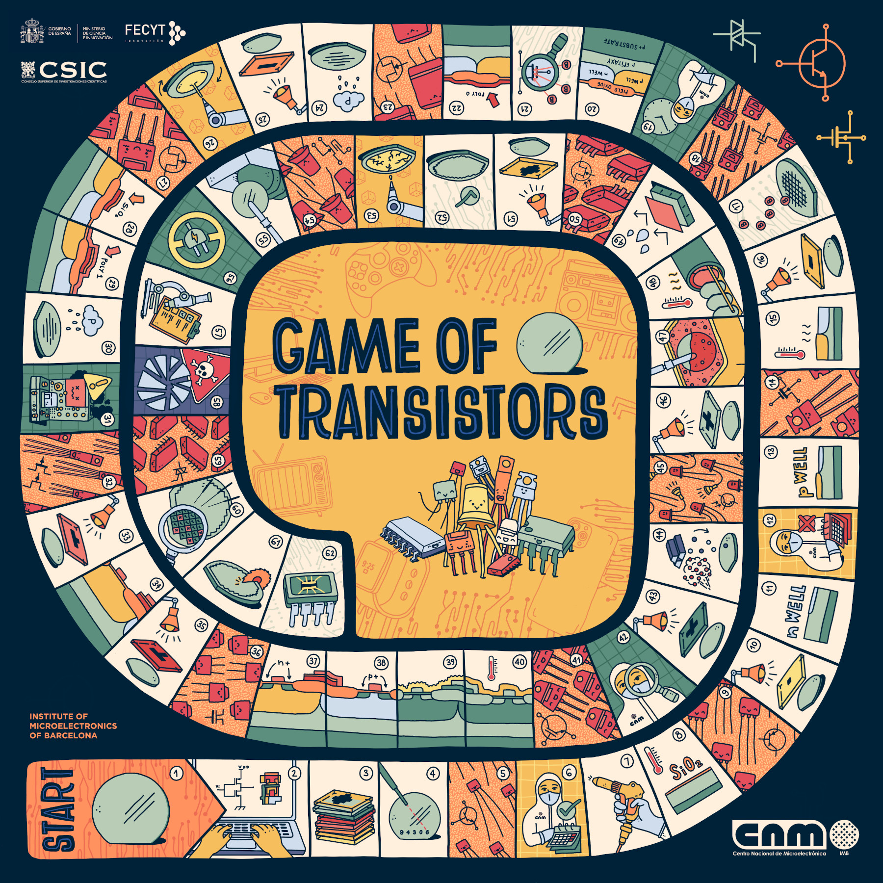 Game of Snakes and Ladders about the manufacture of a MOS transistor, basic element for the manufacture of CMOS circuits, fundamental components of chips. This game allows to follow in a playful way the sequence of steps for its manufacture, including in its cases different "adventures and misfortunes" of a technological process. The game is available with an explanatory guide. It has been specially designed to reach the younger public, to transmit key concepts, such as the manufacturing phases, photolithography, etc. The game starts with a p-type blank wafer and ends with the packaging of the transistor.
The goose squares are different types of transistors:
- 5: BJT NPN Transistor
- 9: BJT PNP Transistor
- 14: NMOSFET Transistor
- 19: PMOSFET Transistor
- 23: NJFET Transistor
- 27: PJFET Transistor
- 32: MESFET Transistor
- 36: HEMT Transistor
- 41: IGBT Transistor
- 45: Photo BJT Transistor
- 50: Photo MOSFET Transistor
- 54: ISFET Transistor
- 59: Thyristor TRIAC Transistor
"De transistor en transistor i tiro perquè passi un electró"
Illustration by Pau Xandri and Alba Teixidor - albateixidor.com
Download Game of Transistors
The History of the Transistor: The Start of the Digital Revolution
If it weren't for the transistor... you wouldn't be here! Did you know that? We explain the history of the transistor and how this small electronic device changed society and everything around us. How much electronics have you used today? And how many transistors?
Fabrication Processes of a Chip: Photolithography
Photolithography is a fundamental process in semiconductor manufacturing. The video explains the steps followed in basic photolithography and what the transfer of the pattern to the wafer surface consists of... we tell you everything you need to know about masks, resist or alignment!
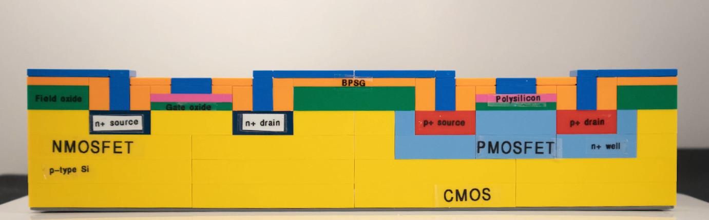
LEGO model of a CMOS process
Three-dimensional model with plastic blocks of different colors that represent the different materials used in the manufacture of a CMOS process with an n-channel transistor (NMOSFET) and a p-channel transistor (PMOSFET). It allows you to visualize the results of the planar manufacturing process used in microelectronics. Made using the well-known LEGO© building block set. You can see the layers of some of the processes that must be carried out for a classic manufacturing process and recognize the layers and materials involved.
Download the flashcard to see the color code and watch the video to learn how to make your own LEGO CMOS!
Educational infographics
Materials made with the collaboration of the Fundación Española para la Ciencia y la Tecnología (FECYT) of the Ministry of Science and Innovation.
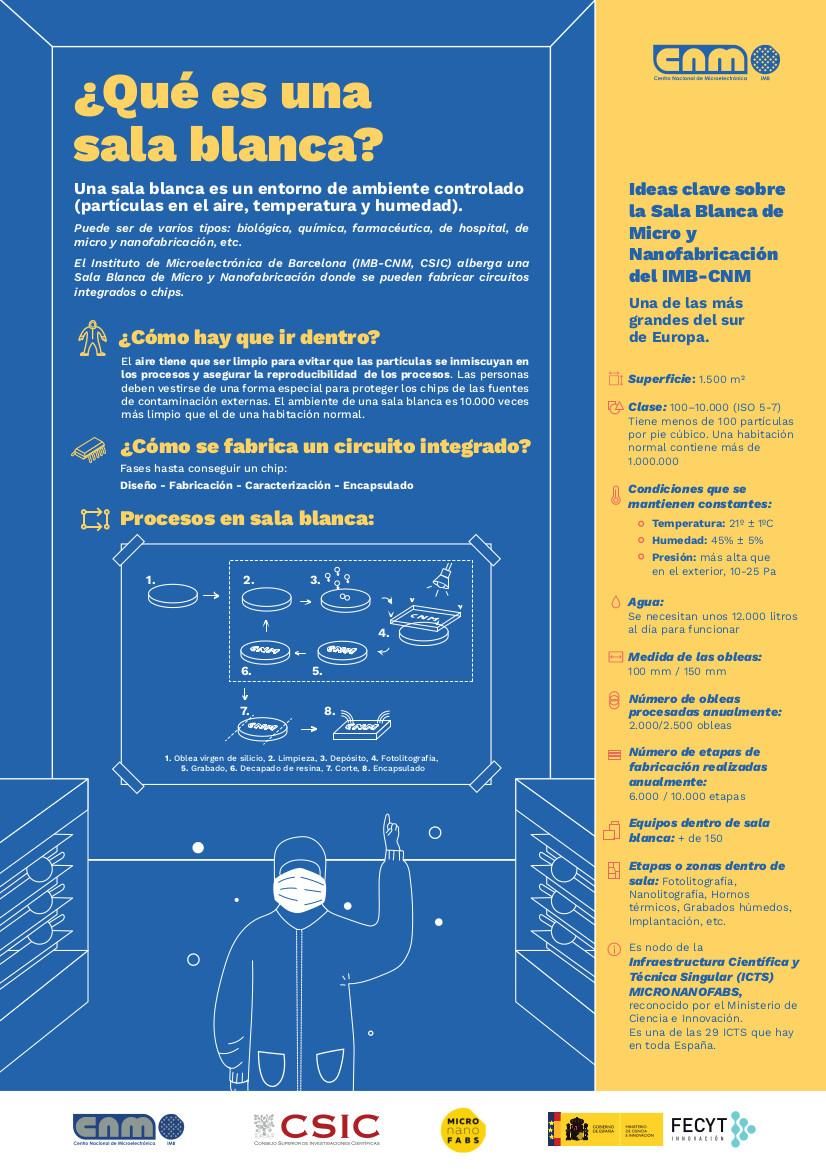
What is a clean room and how does it work?
It illustrates what a clean room is and how a microfabrication clean room like the one at CSIC (recognized as a Unique Science and Technology Infrastructure, ICTS) works. It includes a graphic description of the IMB-CNM's Micro and Nanofabrication Clean Room, one of the largest in southern Europe, the conditions maintained to carry out the work and the processes that take place. The aim is to familiarize the public with cleanrooms, with all the agents involved in their operation and with the microelectronic manufacturing process.
A clean room is a controlled environment (airborne particles, temperature and humidity). It can be of various types: biological, chemical, pharmaceutical, hospital, micro- and nanofabrication, etc. The Institute of Microelectronics of Barcelona (IMB-CNM, CSIC) houses a Micro and Nanofabrication Clean Room where integrated circuits or chips can be manufactured.
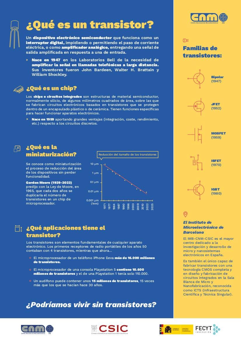
What is a transistor and where can we find them?
It is a graphic support on what a transistor is and how it is integrated into a chip, where transistors are found and what are the most common graphic symbols of the different families. The objective is for the audience to understand what a transistor is and its importance in electronic systems. Could we live without transistors?
The transistor is a semiconductor electronic device that works as a digital switch, preventing or allowing the passage of electric current, or as an analog amplifier, delivering an amplified output signal in response to an input signal. It was born in 1947 at Bell Laboratories from the need to amplify the signal in long distance telephone calls. Its inventors were John Bardeen, Walter H. Brattain and William Shockley.
Design: Xurris & Co.
Clean Room Virtual Tour
Navigate inside the IMB-CNM's Micro and Nanofabrication Clean Room, enter the different workspaces, familiarize yourself with the equipment where wafers are processed, and move around as if it were your own home!
Production: Jotavirtual
Collaboration with FECYT
Some of these materials were produced in the framework of the Un microchip muy grande project (FECYT, ref. FCT-21-16975), organized by the Institute of Microelectronics of Barcelona (IMB-CNM) of the National Spanish Research Council (CSIC) with the collaboration of the Spanish Foundation for Science and Technology of the Ministry of Science, Innovation and Universities (FECYT). Lasting from Summer 2022 to September 2023, it was aimed at improving education and creating scientific vocations among schoolchildren and young non-university people, increasing their learning and interest in electronics and microelectronics. The initiative contemplated different complementary activities: the contest for students “Un microchip muy grande”, the main action; a series of conferences on the history and future of technology, with invited and own presentations; and the exhibition “La revolució silenciosa” that has been exhibited in spaces in Barcelona and Vallès. The initiative celebrated the 75th anniversary of the transistor, a semiconductor electronic device that replaced the bulky and inefficient vacuum tubes of the early 20th century. Initially conceived as an analog amplifier device; Over time, its technology as a digital switch was enhanced and adapted, thus the physical concretion of the '1' and '0' of binary logic.