Equipment and processes of the Photolithography Area
The Photolithography Area is a unique space within the different areas of the Micro and Nanofabrication Clean Room due to the special lighting, temperature and humidity conditions in which it is located. Here the patterns of a mask or reticle are transferred to a substrate by lithographic techniques based on proximity or contact, projection or laser.
Techniques
- Proximity or contact lithography
- Projection lithography
- Direct laser lithography
Equipment
Resist coating and developer equipment
- GAMMA80 Süss automatic pick&place system for coating and developing photosensitive resists on 100 and 150mm wafers (CMOS line).
- One LabSpin6 manual spin coater for positive and negative resists on 50, 100 and 150mm wafers (CMOS line).
- A Delta20 manual Spin coater for positive and negative resists for chips and wafers from 50 to 150mm (CMOS and MNC line available in qualified self-service).
- One Delta80 manual spin coater with Gyrset system for SU8 and transparent polymers for 100mm wafers (CMOS and MNC line available in qualified self-service).
- Two Laurell WS650Mz manual spin coaters for polyimide coating and special processes on chips and wafers from 50 to 150mm (MNC line available in qualified self-service).
- One Laurell WS400A manual spin coater for positive and negative resists for chips and wafers from 50 to 100mm (MNC line available in qualified self-service).
- A GBC 3500 PRO series laminator for ADEX and SUEX processes on wafers from 50 to 150mm (MNC line available in qualified self-service).
- A Laurell WS400A automatic spray developer for 50 to 100mm wafers with OPD4262 developer based on TMAH (MNC line).
- One chemical bench for manual resists developer with deionized water cascade (CMOS line).
- Two chemical benches for manual resists development, one of them with deionized water cascade (MNC line available in qualified self-service).


Lithographic process equipment
- Two manually loaded contact/proximity mask aligners KS MA6/BA6 (g-i line and i-line), with possibility of double-sided alignment and with critical dimension of 1μm on 100 and 150 mm wafers (CMOS g-i line and MNC i-line available in qualified self-service).
- A KS MA150cc contact/proximity mask aligner (LED lamp g-h-i line) with automatic loading and alignment, with the possibility of double-sided alignment and with a critical dimension of 1μm on 100 and 150 mm wafers (CMOS line).
- A Stepper NSR 2205i12D i-line, with critical dimension up to 350nm with maximum exposure range of 22x22mm area for 6''x 6''x 0.25'' reticles on 100 and 150mm wafers (CMOS line).
- A KLOÉ Dilase 650 i-line direct laser lithography system, with 70mw@375nm diode laser and critical dimension of 1μm, with an exposure area range of 3x3 mm2 and with support for DXF,LWI,GDSii formats. (CMOS-MNC line available in qualified self-service).


Resists and polymers annealing and curing equipment
- Seven Heraeus ovens for sample drying and annealing of resists and polymers (4 for CMOS Line and 3 for MNC Line)
- One Ovenvan oven with nitrogen flow and temperature ramp programming for polyamide curing (MNC Line)
- Three hotplates for sample drying and annealing of resists and polymers (MNC Line available in qualified self-service)
- One JP Selecta programmable hot plate for SU8 curing ramps (MNC Line available in qualified self-service)
- Two UV curing equipment (CMOS and MNC Line available in qualified self-service)
Wafer and mask cleaning equipment
- One OEM Group R&D with touch screen for 100mm wafers (CMOS Line)
- Two R&Ds Semitool for 100mm wafers (MNC Line) and 150mm wafers (CMOS Line)
- One OBDUCAT QS W 300SM automatic mask cleaning system for 5x5 and 7x7 inch masks, using pyranha and RCA1 mix, incorporating Megasonic and including rinsing and drying (CMOS Line).


Available capabilities
- Optical lithography using positive and/or negative resists for wet and dry etching and ion implantation. Chips and substrates from 50 to 100mm.
- Patterning by means of LOR and AZ resists for lift-off processes.
- Micro and nano designs by Stepper.
- Microfluidic structures and molding with SU8 and SUEX/ADEX.
- Structural layers with polyamide.
- Prototyping with Direct Laser Writer.
- User training for qualified self-service.
Download the tecniques and capabilities of the Photolithography Area
Check the Photolithography Area
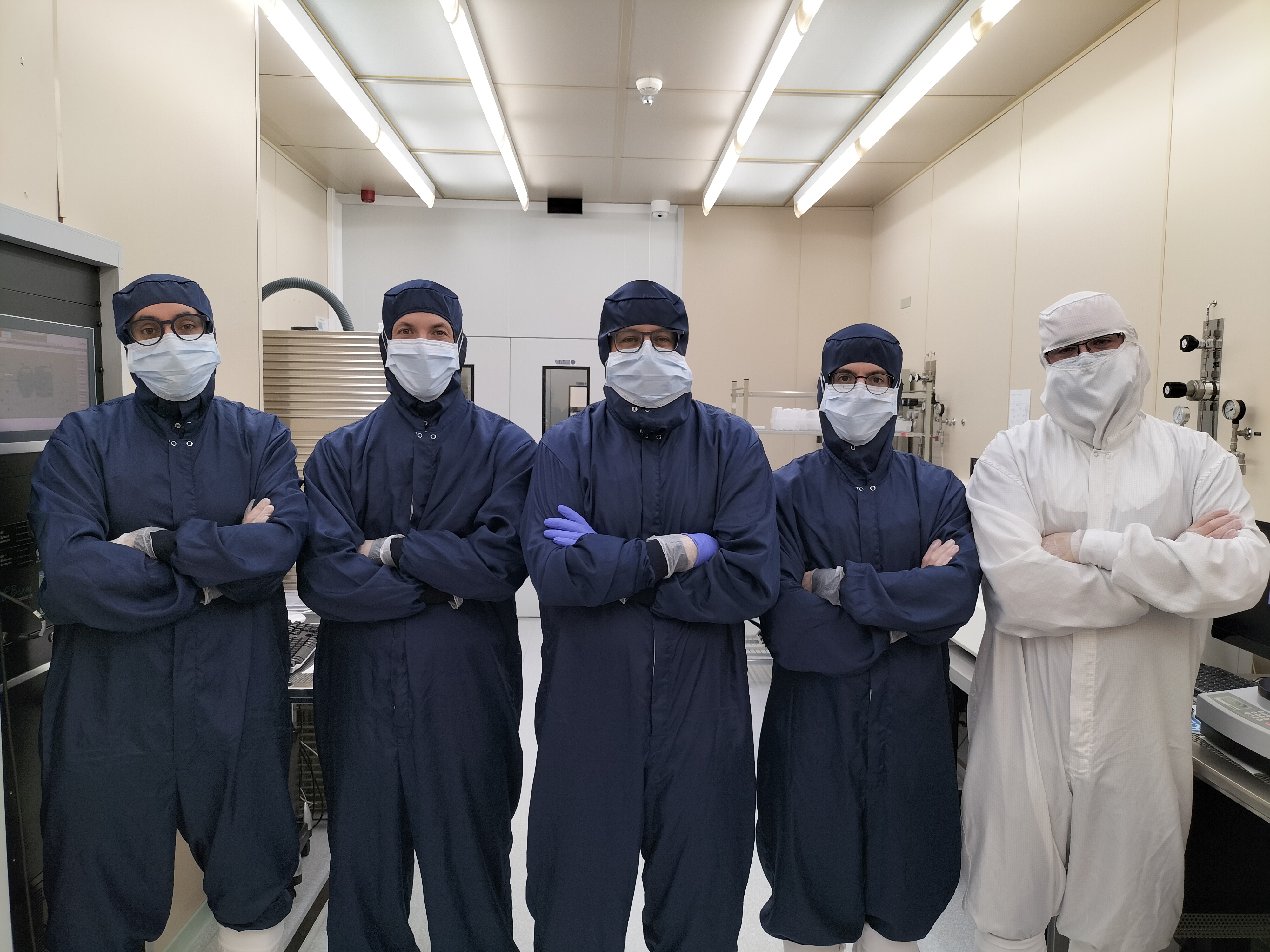
Photolithography Team
- Javier Sánchez (Ext. 435560)
- Luis Rull (Ext. 435689)
- Héctor Cabezas (Ext. 435574)
- Alberto Del Moral (Ext. 435672)
- Albert Guerrero (Ext. 435562)