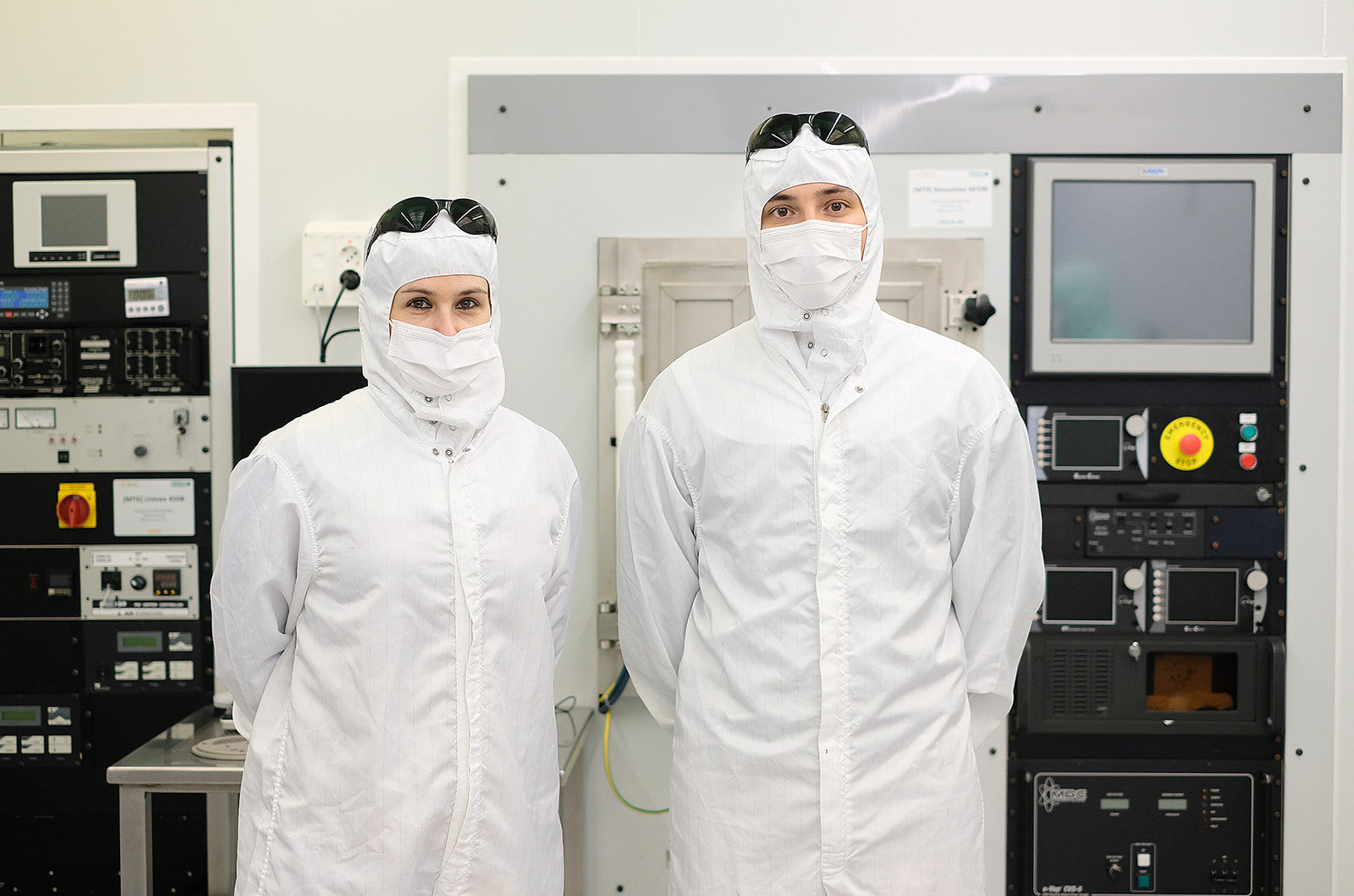
Equipment and processes of the Metallization Area
The Metallization Area is the area where metal thin films of a variety of materials can be deposited by Physical Vapour Deposition techniques on either DC and DC/RF sputtering systems, or on thermal and e-beam evaporation systems.
Techniques
- Physical Vapor Deposition on Sputtering Systems (DC and DC/RF)
- Physical Vapor Deposition on Evaporation and E-Beam Systems
Equipment and Available capabilities
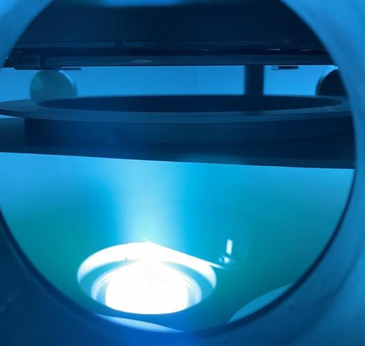
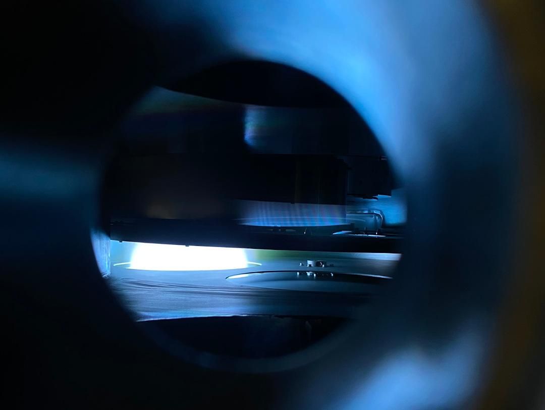
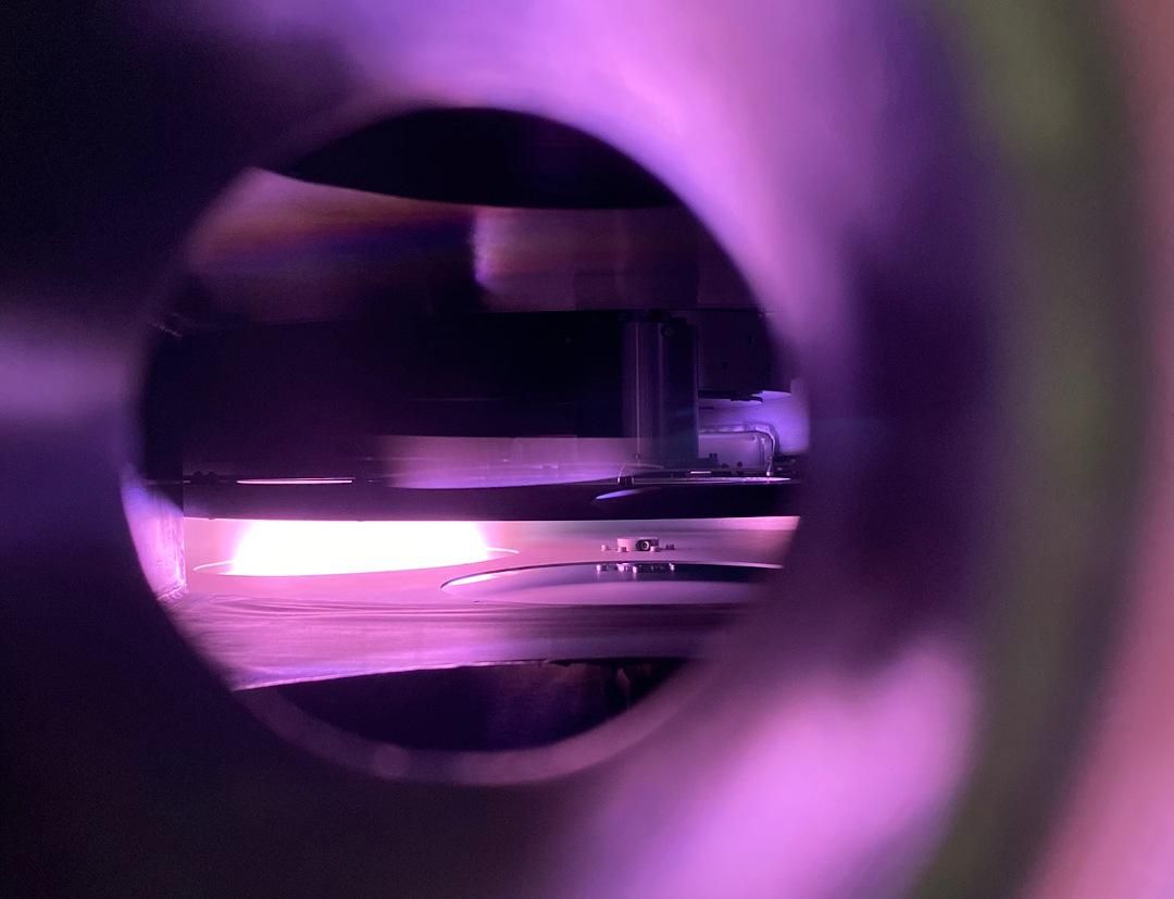
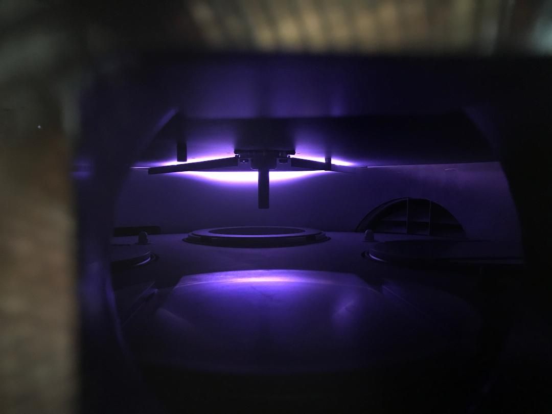
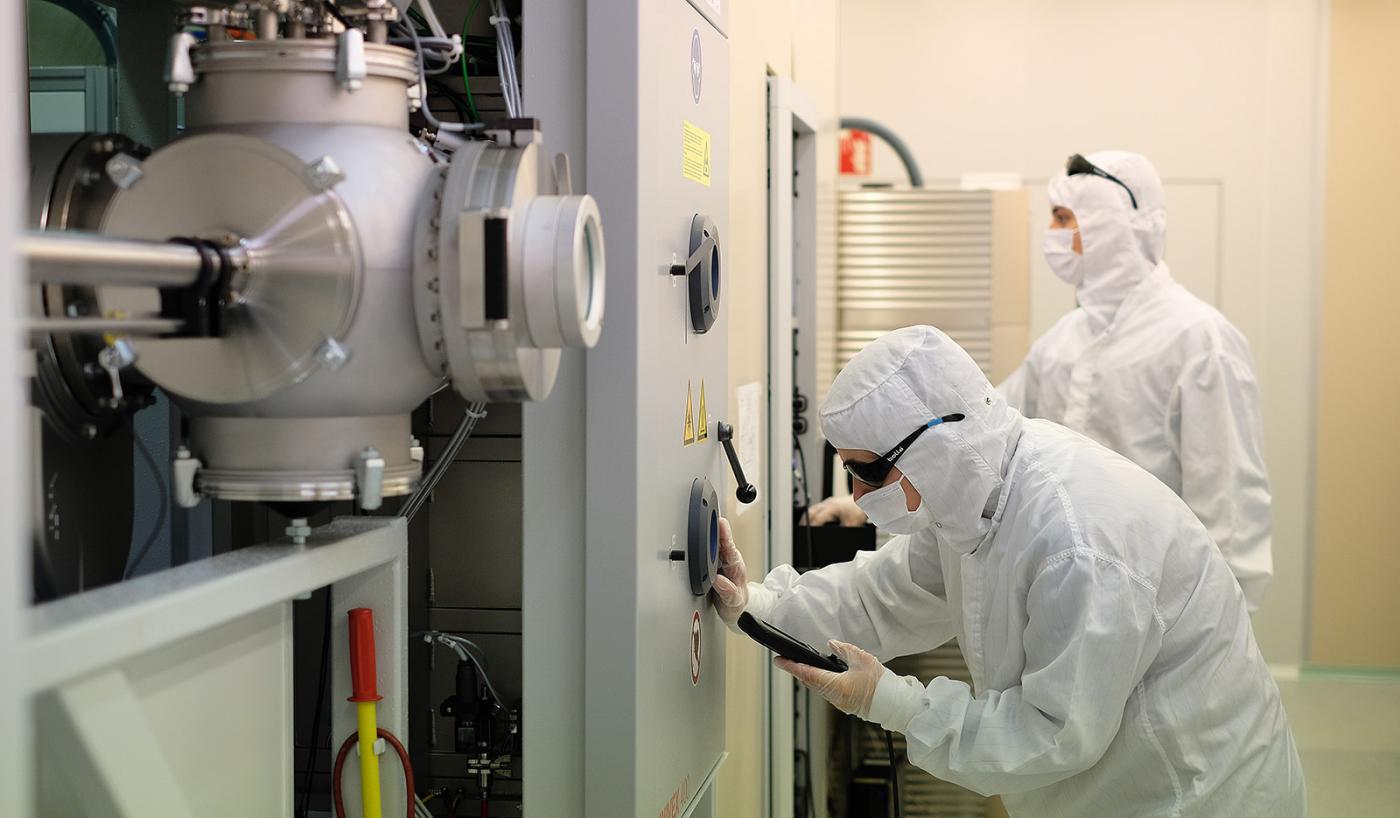
Physical Vapor Deposition on Sputtering Systems
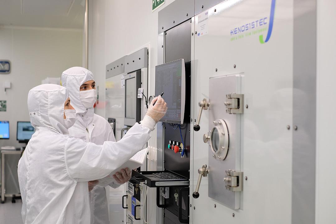
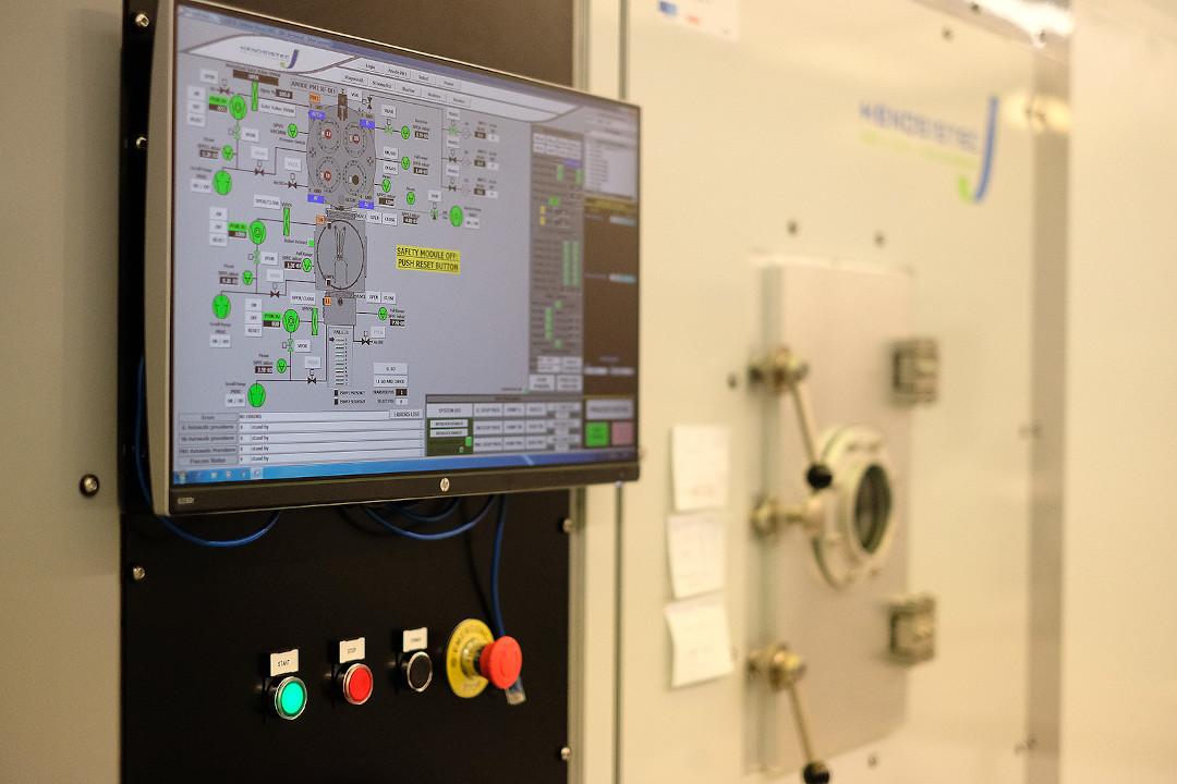
KENOSISTEC KS800H:
- Sputtering system to deposit metallic layers on 100 mm or 150 mm wafers.
- Process chamber with three (200 mm) circular planar magnetron cathodes.
- Available targets: Al99.5/Cu0.5, Ti and Cu.
- Load lock chamber with semi-automatic loading system.
- DC power and RF for sputter etching.
- Possibility to process CMOS or no-CMOS wafers (no-CMOS without etching).
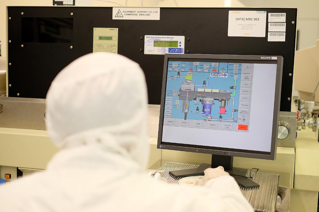
Material Research Corporation-MRC 903:
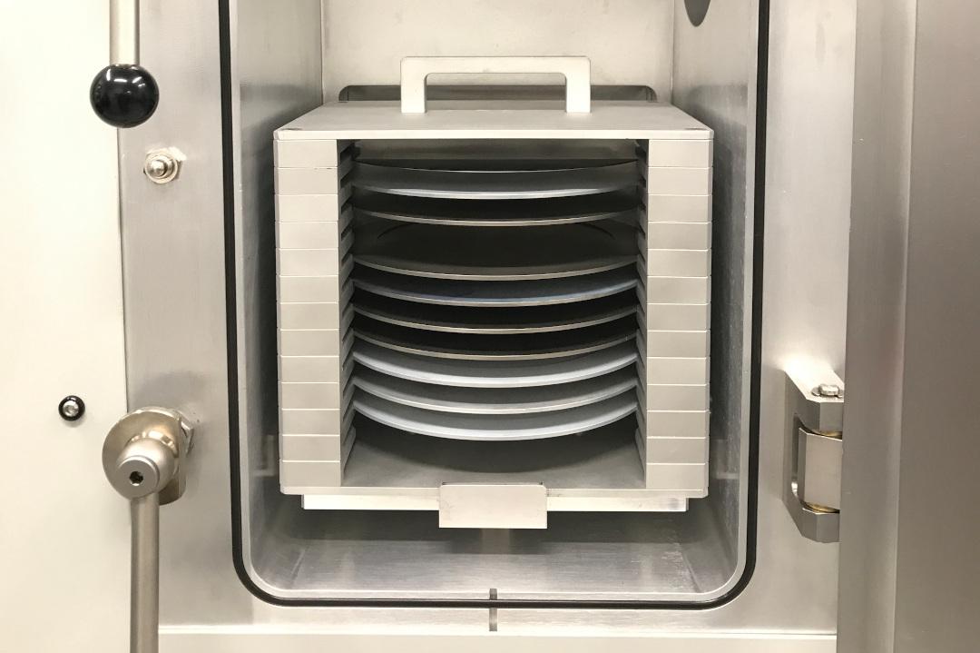
- Sputtering system to deposit metallic layers on a 30 x 30 cm2 pallet surface (up to nine 100 mm wafers or up to four 150 mm wafers).
- Process chamber with three cathodes (two are rectangular planar magnetron-type and the other is a rectangular planar diode).
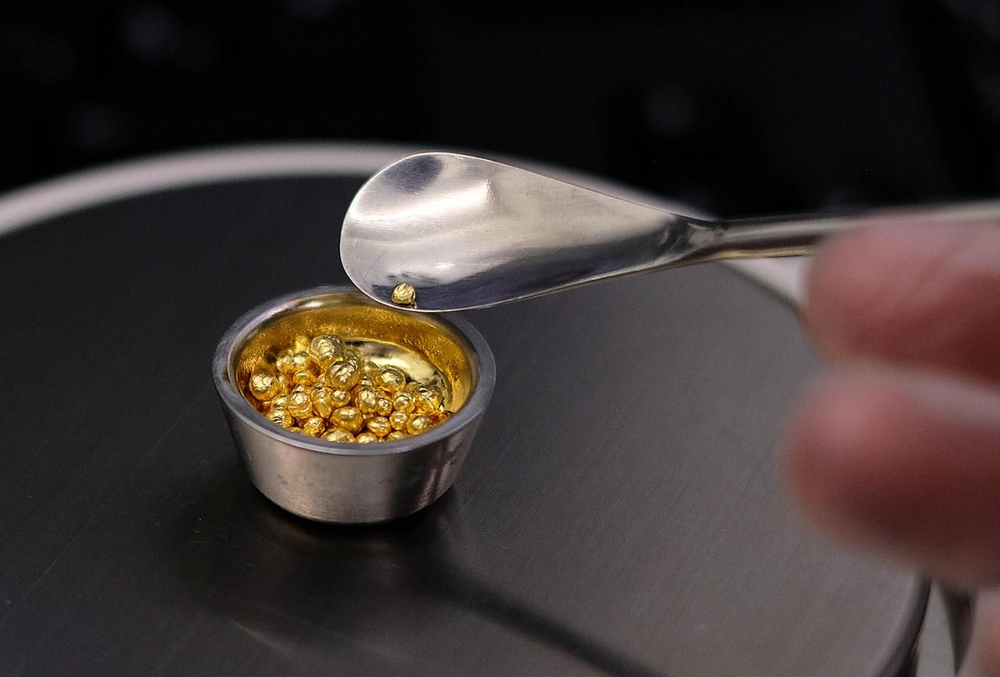
- Available targets: Au, Ni and Ti.
- Load lock chamber with semi-automatic loading system.
- DC power for Ti/Ni and RF power for Au. Also RF for sputter etching.
- Aimed at no-CMOS wafers.
KENOSISTEC KS500C:
- Sputtering system to deposit metallic and semiconducting layers on 100 mm or 150mm wafers.
- Process chamber with three cathodes (75 mm) magnetron circular planar in confocal configuration.
- Available targets: W, Ti, Ta, Si and TaSi2
- Load lock chamber with semi-automatic loading system.
- DC power supply source plus RF power supply for one cathode (to deposit Si). Possibility to sputter etching (RF).
- Possibility to process CMOS and no-CMOS wafers (no-CMOS without etching).
LEYBOLD HERAEUS Z-550:
- Sputtering system to deposit metallic layers on 100 mm wafers.
- Process chamber with a circular planar magnetron cathode.
- Available targets: Al, Al98.75/ Cu0.5 /Si0.75 and TaSi2.
- Load lock chamber and manual loading system.
- DC power supply source. Possibility to sputter etching (RF).
- Possibility to process CMOS or no-CMOS wafers (no-CMOS without etching).
KENOSISTEC KS800HR:
- Sputtering system to deposit metallic and non-metallic layers on 100 mm, 150 mm wafers.
- Process chamber with four (200 mm) circular planar magnetron cathodes.
- Available targets: Al, Al99.5/Cu0.5, Ti, W, Si, AlN, TiN, Si3N4, SiO2
- Load lock chamber with semi-automatic loading system.
- Possibility to heat samples up to 400 ºC
- Pulsed DC and RF power supply sources, plus RF for sputter etching.
- To process no-CMOS samples
BIO RAD E-5000 Polar Division:
- Sputtering system to deposit gold layers for scanning electron microscopy.
- Possibility to change distance and current.
- Stopwatch to time control.
Physical Vapor Deposition on Evaporation and E-Beam Systems
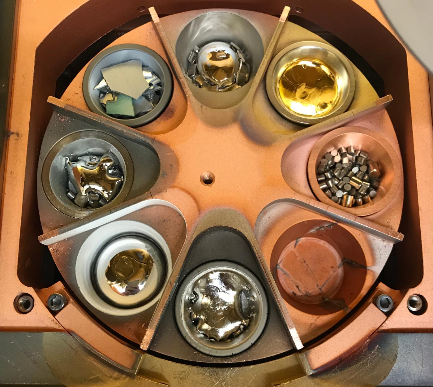
OERLIKON UNIVEX 450B:
- One electron gun source with four pockets and two thermal sources.
- Maximum sample area size: 150 mm.
- Process chamber capacity up to four wafers (Manual loading system without load lock chamber)
- Available materials: Ag, Al, Al2O3, Au, B, C, Cr, Cu, Fe, ITO, Mo, Nb, Ni, Pd, Pt, Sn, Ta, Ti, W, ZnO and Zr.
- Possibility to heat samples up to 500ºC.
- Residual gas Analyzer.
- Available deposition in low O2 pressure.
- To process no-CMOS samples.
KENOSISTEC KE500E:
- One electron gun source with four pockets.
- Maximum sample area size: 150 mm.
- Process chamber capacity limited to one wafer (manual loading system without load lock chamber).
- Available materials: Al, Cr, Ti.
- Exclusively to process CMOS samples.
LEYBOLD UNIVEX 400:
- One electron gun source with eight pockets
- One i-gun source.
- Maximum sample area size: 150 mm.
- Process chamber capacity of one wafer with load lock chamber.
- Possibility to cool samples between -20 and 100 ºC.
- Possibility to sample rotation during deposition
- Available materials: In test: (Ti, Au, Al)
- To process no-CMOS samples.
Download the tecniques and capabilities of the Metallization Area
Check the Metallization Area
Metallization Team
- Leyre Martínez de Olcoz Sainz (ext. 435563)
- Josep Montserrat i Martí (ext. 435553)
- Marc Isart Alemany (ext. 435690)