Equipment and processes of the Dry Etching Area
The Dry Etching Area is the area where plasma etching techniques are carried out on different materials used in microfabrication.
Techniques
- Metal etching
- Semiconductors
- Polymers
- Deep silicon etching with HAR
- Etching for silicon nanostructures
Equipment and Available capabilities
Alcatel 601 E
- Automatic single-wafer up to 100 mm
- ICP Gen. up to 2000 W - 13,56 MHz
- RF Gen. up to 500 W - 300 KHz
- Gas lines: SF6, C4F8, He, O2
- 2 mechanical pumps 2 turbomolecular pumps
- Wafers thermalization: -110°C to 40°C (N2 dewar); He-backside contact
- Bosch process
- Layer etching: Silicon, polysilicon, W and TaSi
OXFORD PLASMALAB S-100 no CMOS
- Automatic multiwafer up to 100 mm. Two chambers
- ICP Gen. to 5000 W-2 MHz and ICP Gen. up to 3000 W-13.56 MHz
- RF Gen. up to 600 W-13,56 MHz
- Gas lines: N2, O2, He, SF6, Cl2,.
- Chamber 1: HBr, BCl3, Cl2, SF6, N2, He, Ar
- Chamber 2: SF6, O2
- 3 mechanical pump 2 turbomolecular pump
- Wafers thermalization: 20°C to 60°C; He-backside contact
- Layer etching: Group III-V compound semiconductors, SiC, diamond and photoresist stripping


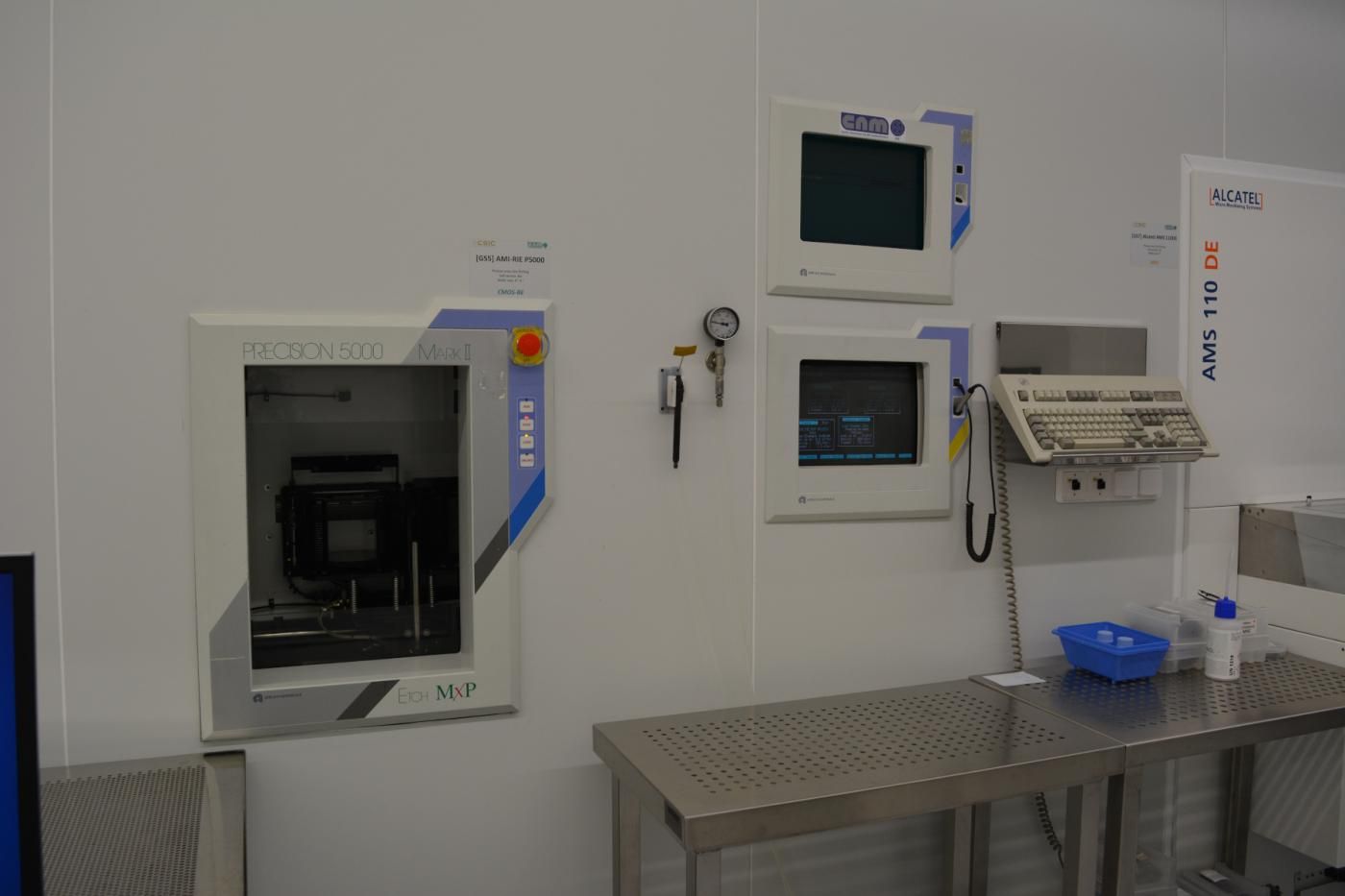
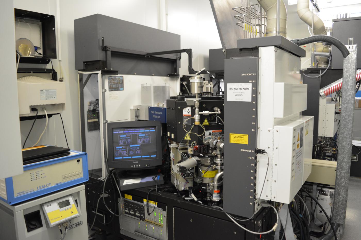
Aplied Materials P5000
- Industrial platform 3 chambers up to 150 mm
- Magnetic field assisted, up to 90G – MERIE
- 3 RF Gen. up to 1250 W - 13,56 MHz
- 3 mechanical pumps 3 turbomolecular pumps
- Gas lines:
- Chamber A: CF4, C2F6, He, CHF3, Ar
- Chamber B: C4F8, CF4, C2F6, O2, He, CHF3, Ar
- Chamber C: HBr, Cl2, CF4, He/O2, SF6, N2
- Layer etching: Polysilicon, SiO2, Si3N4
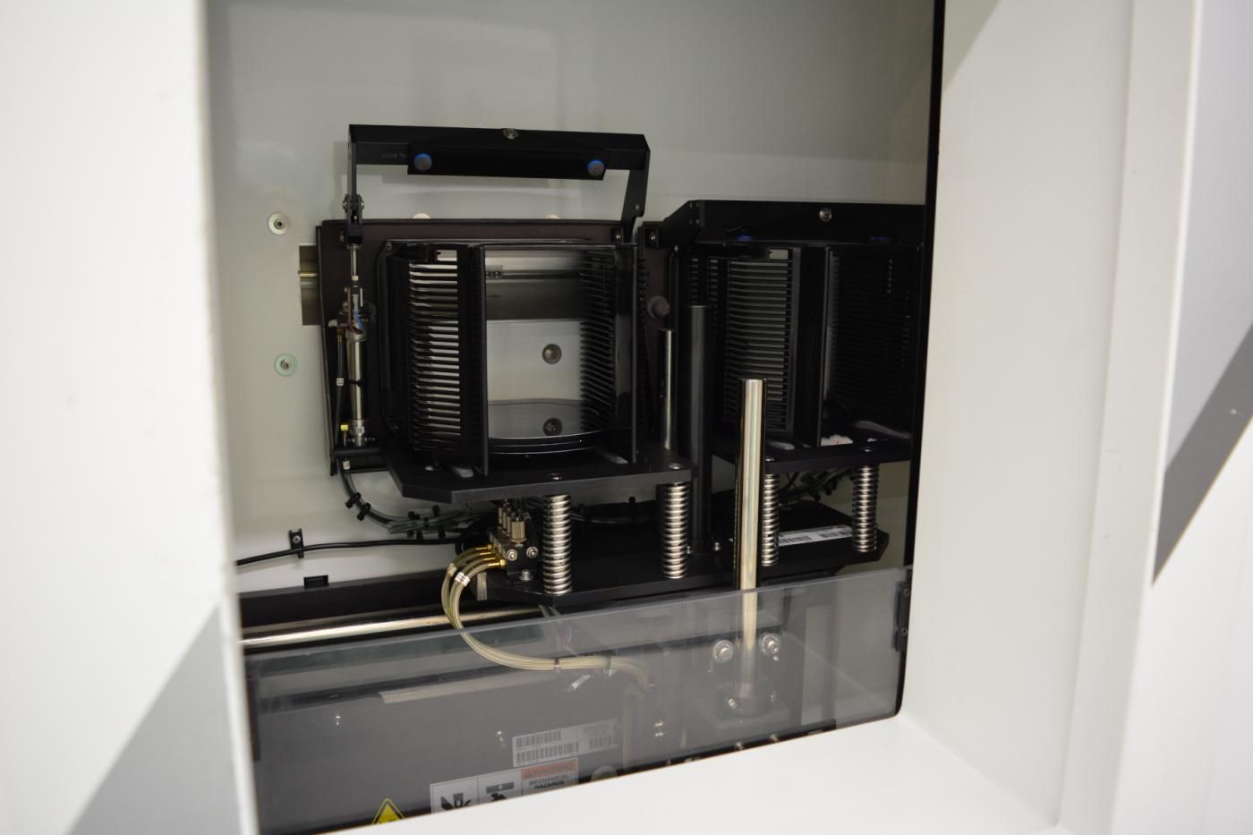
Alcatel AMS-110 DE no CMOS
- Automatic single-wafer up to 100 mm
- ICP Gen. up to 3000 W - 13,56 MHz
- RF Gen. up to 600 W - 300 KHz
- RF Gen. Up to 500 W LF
- Gas lines: SF6, C4F8, He, O2 CH4, Ar
- 1 mechanical pumps 1 turbomolecular pumps
- Wafers thermalization: -10°C to 420°C; He-backside contact
- Bosch process
- Layer etching: Silicon, polysilicon, W, TaSi, SiO2, Si3N4, Al2O3, HfO2, TiO2, GaO, pyrex, polyimide, Graphene

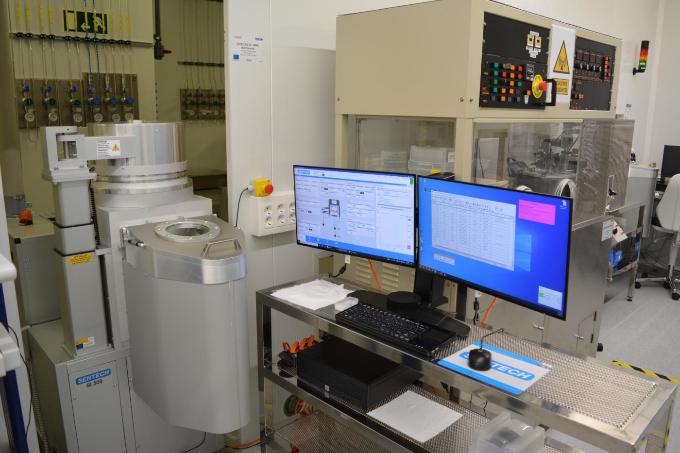
SENTECH SI 500 No CMOS
- Automatic single-wafer up to 150 mm MNC
- ICP Gen. up to 2000 W - 13,56 MHz
- RF Gen. up to 600 W – 13,56 MHz
- Gas Lines: SF6*, C4F8*, CF4, O2*, He, Ar. (* Duplicate massflows)
- 2 mechanical pump 1 turbomolecular pumps
- Temperature: -15ºC up to 80ºC. He-backside thermalization
- Bosch process
- Layer etching: Silicon, SiO2, Si3N4, polyimide, graphene
SENTECH SI 500 SI
- Automatic single-wafer up to 150 mm MNC
- ICP Gen. up to 2000 W - 13,56 MHz
- RF Gen. up to 600 W – 13,56 MHz
- Gas lines: SF6*, C4F8*, O2*, He, Ar. (* Duplicate massflows)
- 2 mechanical pump 1 turbomolecular pumps
- Temperature: -15ºC up to 80ºC. He-backside thermalization
- Bosch process
- Layer etching: Silicon, SiC
SENTECH SI 500 CL
- Automatic single-wafer up to 150 mm MNC
- ICP Gen. up to 2000 W - 13,56 MHz
- RF Gen. up to 600 W – 13,56 MHz
- Gas Lines: Cl2, BCl3, Ar, N2, O2, He
- 2 mechanical pump 1 turbomolecular pumps
- Temperature: -15ºC up to 80ºC. He-backside thermalization
- Optical end point detection
- Layer etching: Group III-V compound semiconductors
ALCATEL GIR 160
- Parallel plate RIE manual single wafer up to 150 mm
- RF Gen. up to 500 W – 13,56 MHz
- Gas lines: SF6, CHF3, CF4, O2, He, N2
- 1 mechanical pump 1 turbomolecular pump
- No control temperature
- Layer etching: Silicon, Polysilicon, SiO2, Si3N4, SiC, TaSi


Download the tecniques and capabilities of the Dry Etching Area
Check the Dry Etching Area
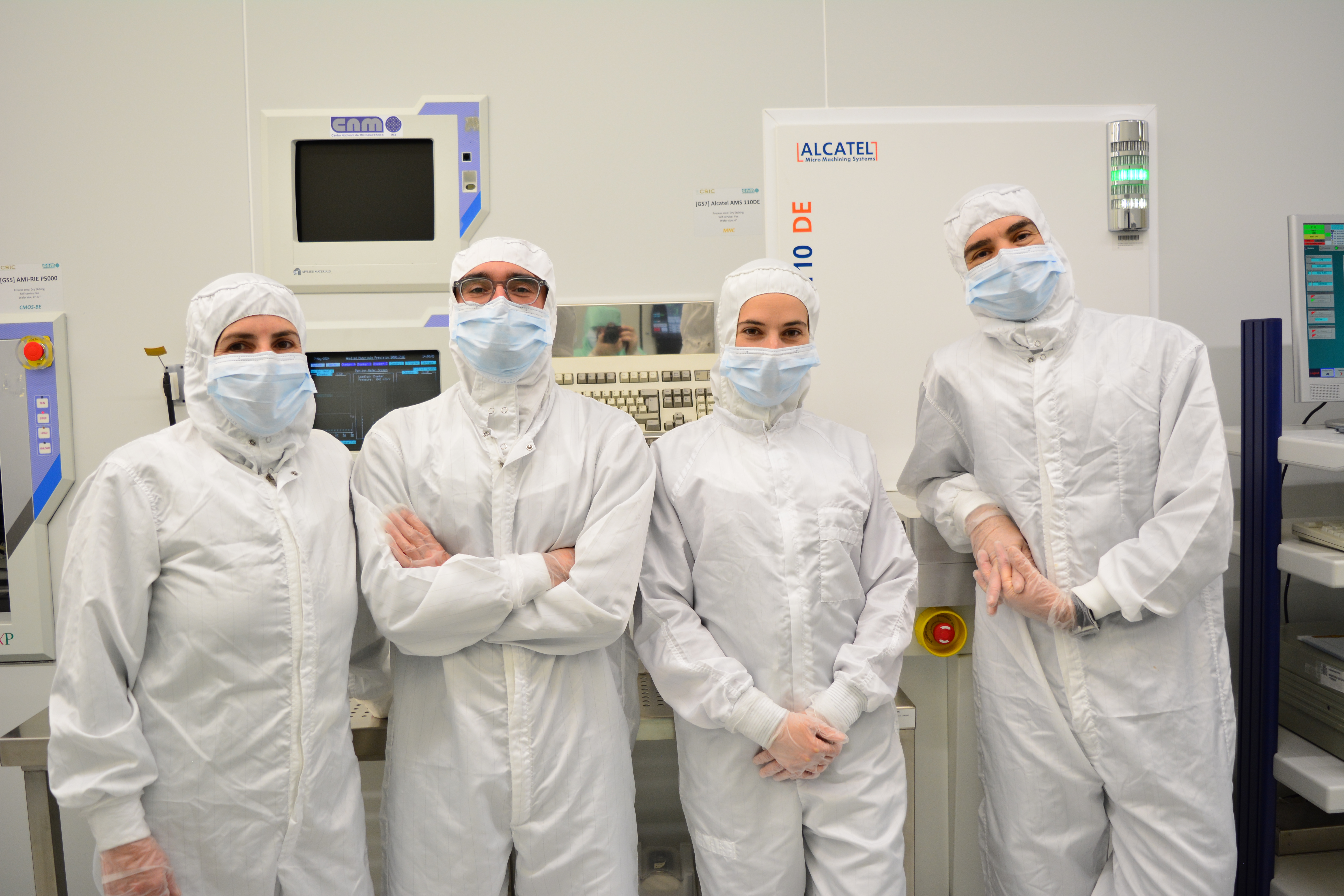
Dry Etching Team
- Roser Mas (ext. 435570)
- Carles Mateu (ext. 435569)
- Guillem Ropero (ext. 435571)
- Yannick Sornoza (ext. 435579)