


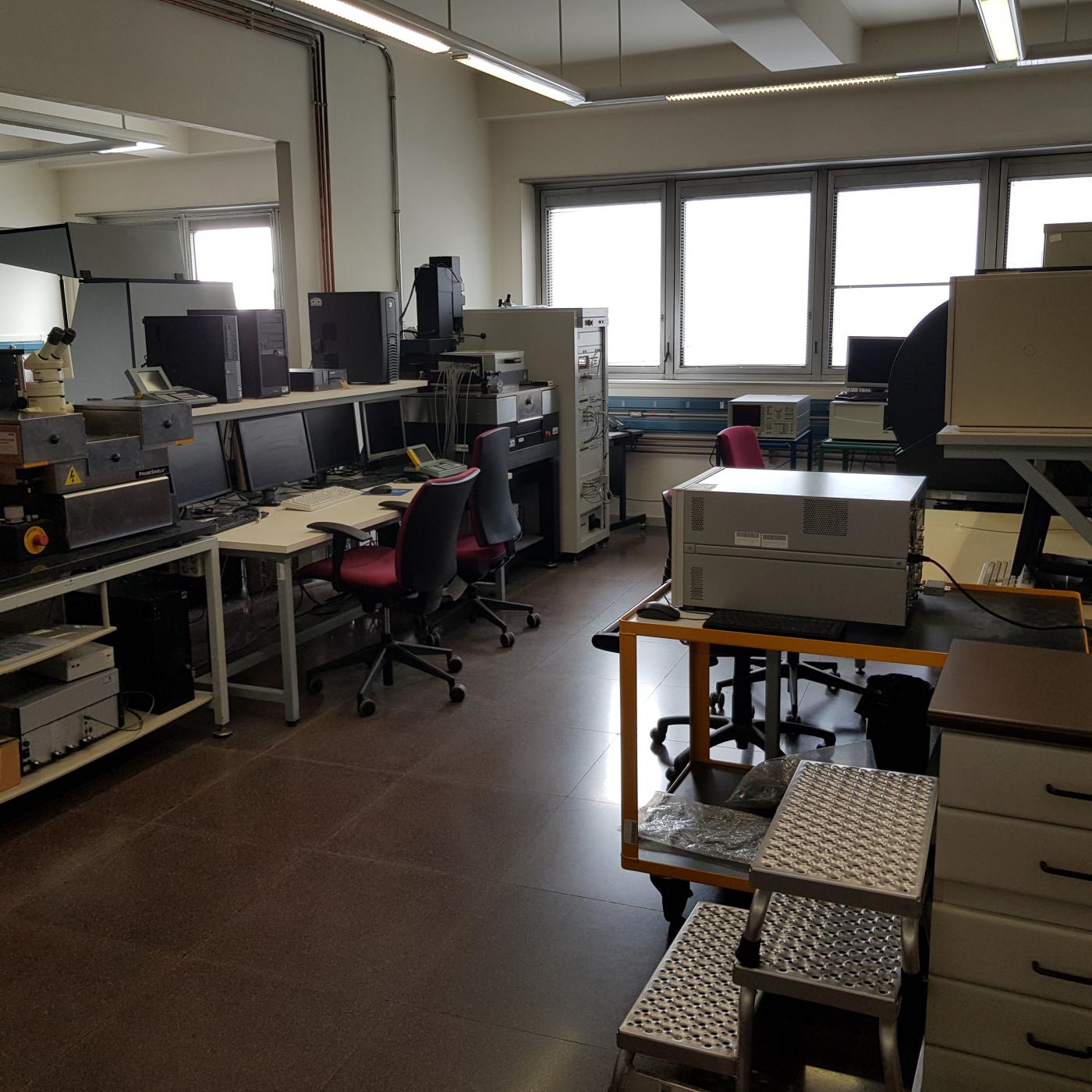
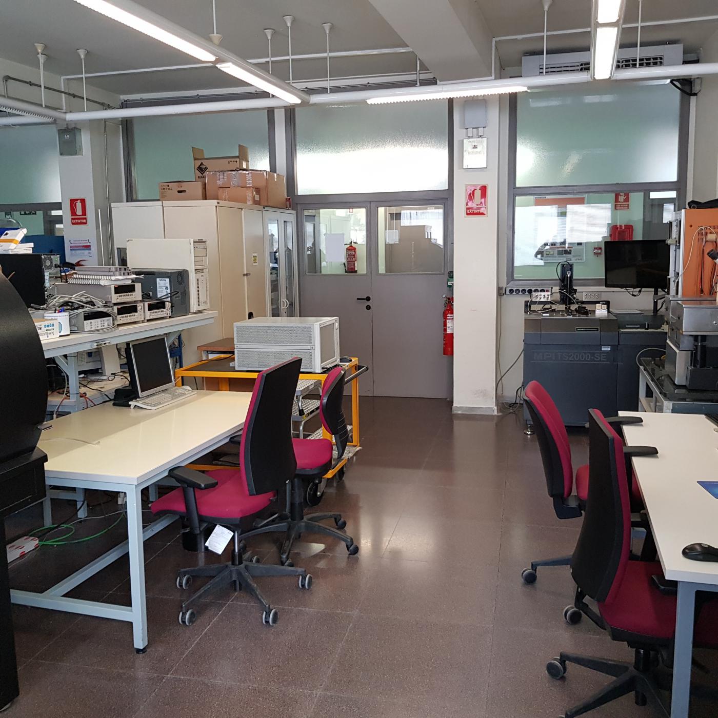
Wafer Electrical Characterization Laboratory
The main activities of this service deal with:
- Parametric test
- Test structure design and characterization
- New on-wafer measurement techniques set-up
- Electronic Device Characterization
Equipment
Parametric test system
Semi-automatic parametric test station, based on a Süss Microtech PA200 semi-automatic prober and an Agilent 41000 Parametric Test System. It has 4 SMU units, a CV meter and a switching matrix. Connection to the wafer is done through probecard.
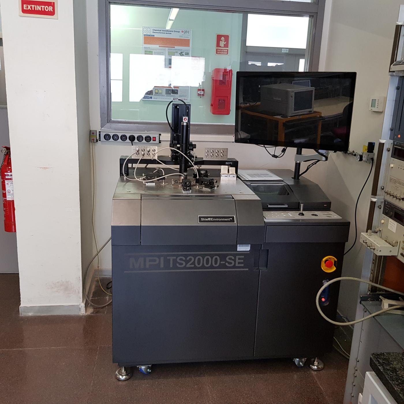
Probers
Apart from the parametric testing system, we have 4 semi-automatic prober machines available:
- MPI TS2000-SE
- Wentworth AWP 1050 (Clean Room)
- KarlSüss PA200
- MPI TS2000-SE thermal (-40 ºC to 300 ºC)
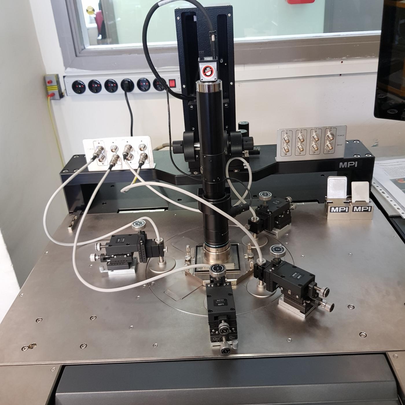
It can be contacted on wafer or chip using micro manipulators or prober card.
General purpose on-wafer measurement equipment
These probers can be used together with the available electrical measurement equipment:
- 4 semiconductor parameter analysers:
- Keysight B1500
- HP4155B
- 2 Keithley 4200, both include 4 SMU and one with CV module
- CV measurement equipment:
- Keysight E4990
- HP4280A
- HP4192A
- Other small auxiliary equipment such as Keithley 2600, Keithley 2470, etc.
Contact
Sergi Sànchez