Power Devices and Systems Group (PDS)
The Power Devices and Systems Group focuses on the design, fabrication, characterization and integration of power semiconductor devices, optimized for developing reliable and energy efficient converters and electronic systems, operating even in harsh environments (high temperature, radioactive environments, etc.).
Contact Person
Dr. Miquel Vellvehi
More info

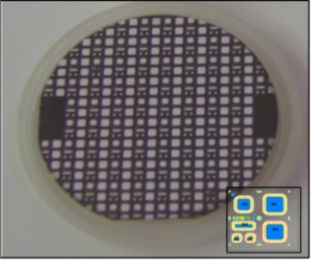
The devices are developed on different semiconductors (Si, SiC, GaN), and fabricated in the Clean Room of the IMB-CNM, covering various application fields (traction, protection, high frequency, space, high energy, etc.). The Group has three main research lines: Silicon Power Devices, Wide Bandgap Semiconductor Devices and Power Systems Integration and Reliability.
Silicon Power Devices
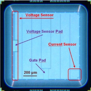
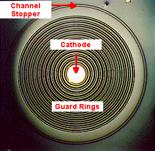
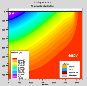
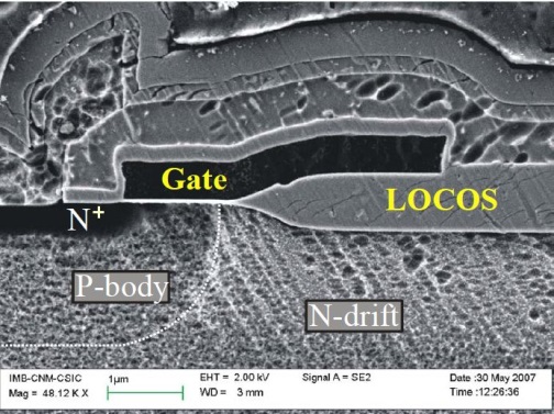
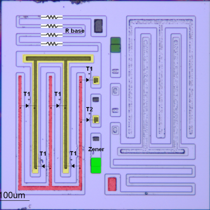
- High voltage devices for robust and energy efficient high voltage converters and smart distribution networks. Intelligent 2.5 to 6.5 kV IGBTs with monolithically integrated voltage and current sensors and advanced high voltage MOS-Thyristors.
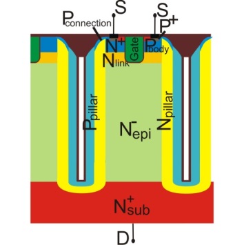
- High voltage Super-junction MOS transistors for DC/DC converters and power factor correction and LDMOS transistors for RF applications.
- Protection devices for domestic and telecommunication applications and AC switches for lighting and thyristor firing.
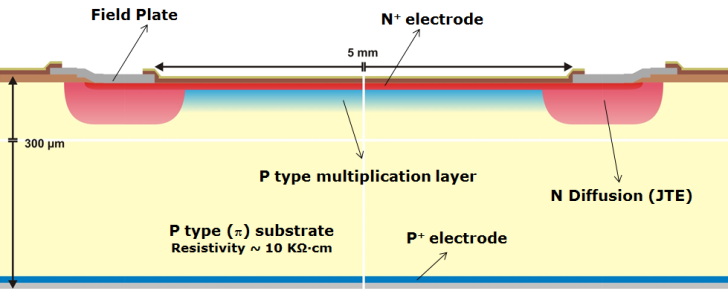
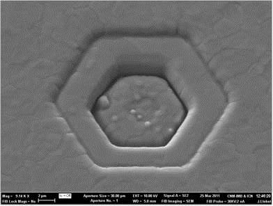
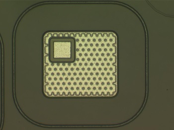
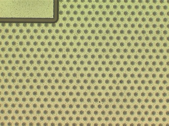
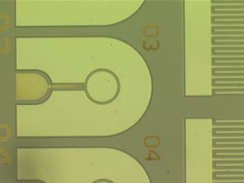
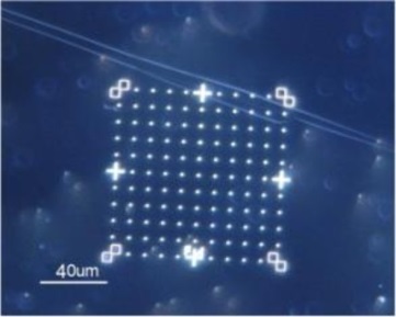
- Design and fabrication of Low Gain Avalanche Detectors (LGAD) for high energy physics and medical applications
Wide Bandgap Semiconductor Devices
- Optimized process technologies for wide bandgap semiconductors: silicon carbide (SiC), gallium nitride on silicon (GaN on Si) and more recently diamond.
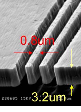
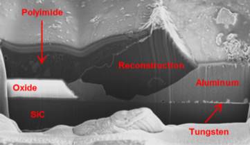
- Design, fabrication and characterization of new power devices based on these materials for high-voltage and high temperature applications. In SiC, focus is on gate-controlled MOS structures, JFET devices and very high voltage diodes (> 5kV). In GaN, focus is on MIS-HEMT devices, which have significant potential in the 600V application range, such as electric car and power supplies.
- Fabrication of high-temperature devices (diodes, switches, integrated circuits) for aeronautical and space applications.
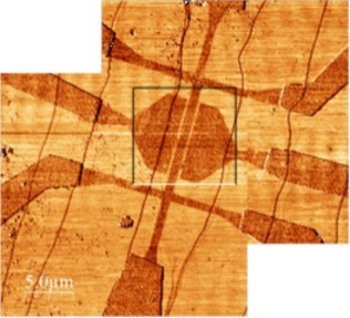
- Study of carbon-based materials as, for example, epitaxial graphene on SiC or carbon nanotubes.
Power Systems Integration and Reliability
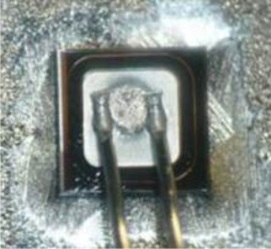
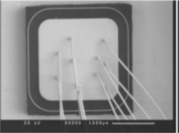
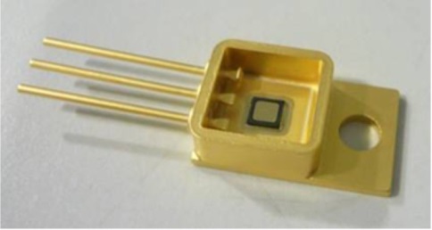
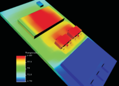
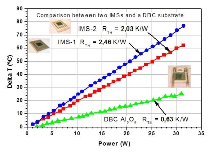
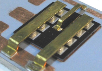
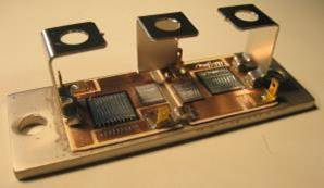
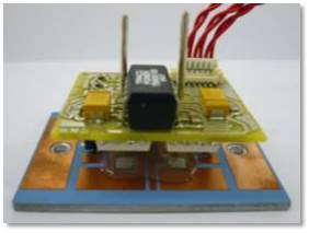
- Design of new modules and discrete packages based on 3D thermal simulation. Thermal characterization, modeling and parameter identification of the systems developed.
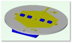
- Design and development of packaging solutions for highly integrated power modules with improved features of power management, temperature, switching speed and reliability.
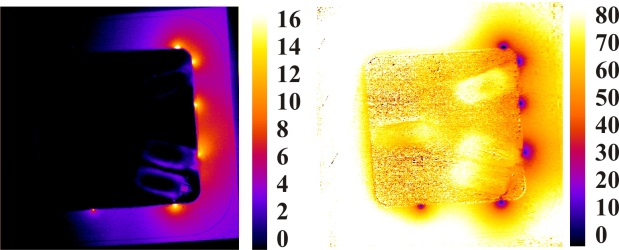
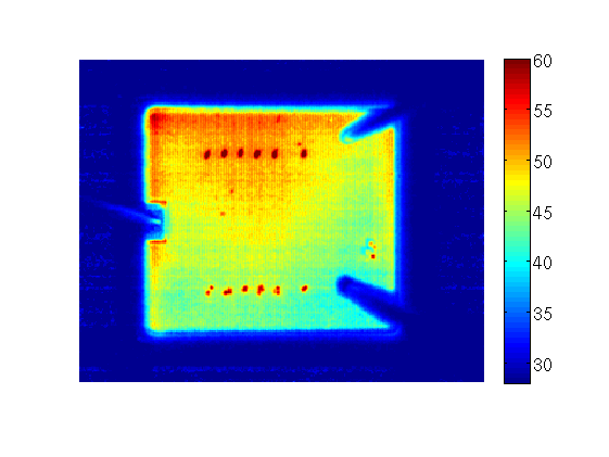
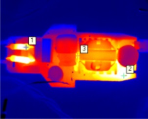
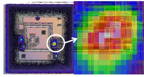
- Advanced Electro-Thermal Characterization based on optical and infrared methods at chip and system level.
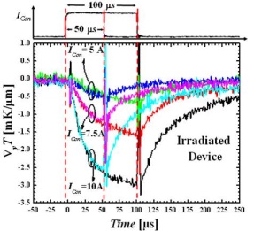
- New methodologies for the analysis of the operation limits and reliability of advanced power systems and devices.