Integrated Circuits and Systems Group (ICAS)
The essence of this group has been always the design of application specific integrated circuits (ASICs). Currently, ICAS R&D is focused on ultra low-power analog, mixed and RF integrated circuits, organic/printed microelectronics, short range RF communications with remote power systems, digital integrated circuits in nano-electronics and multi-technological HDL-AMS modeling. The group also supports electronic system design for the ICAS itself as well as for other R&D groups of IMB.
Contact Person

The overall objective of the ICAS group is addressing new technologies, techniques and architectures to improve the performance of integrated circuits and systems, exploring the continuous advances of "micro/nano-electronic" devices and promoting their usage and exploitation in real "macro" application fields. In this sense, the use of advanced technologies, such as nano-CMOS, M/NEMS, MCM, 3D-packaging and "printed-electronics" are studied for the best performance-cost compromise when facing new design projects. In this framework, we can classify the specific objectives of the ICAS group according to three main R&D lines:
Low-power analog CMOS integrated circuits
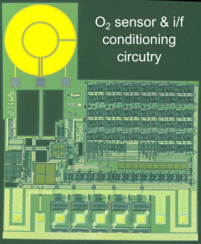
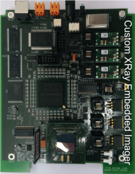
- Hybrid image sensors (detector + read-out integrated circuit) and the external electronic systems for image processing (X-ray, Infrared and visible spectrum)
- Circuits and systems for biomedical applications (hearing-aids, pacemakers...)
- Monolithic A/D interfaces for smart sensors (N/MEMS and chemical sensors)
- RF interfaces for short-range communications and remote powered devices
System integration and development based on flexible platforms
- ASIC/FPGA-design including Hw/Sw and short-range communications (Bluetooth, Zigbee, NFC)
- Development of systems-on-chip (SoC) based on flexible platforms and virtual components
- Modeling and simulation of multi-technology systems
Organic, printed and flexible electronics
- Development, characterization and modeling of these new technologies
- Development of device and cell libraries and the corresponding design-kits
- New design methodologies, flows and EDA tools customization
- Design application specific "printed- electronics" circuits