


Silicon Nitride Photonic Integration Platform
A fabrication process on Silicon Nitride technology has been developed in collaboration between IMB-CNM and VLC Photonics, providing a stable and scalable photonics manufacturing platform with a mature process design kit and component libraries.
Overview
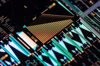
The Silicon Nitride Platform, runs in the microfabrication facility housed in the IMB-CNM Clean Room.
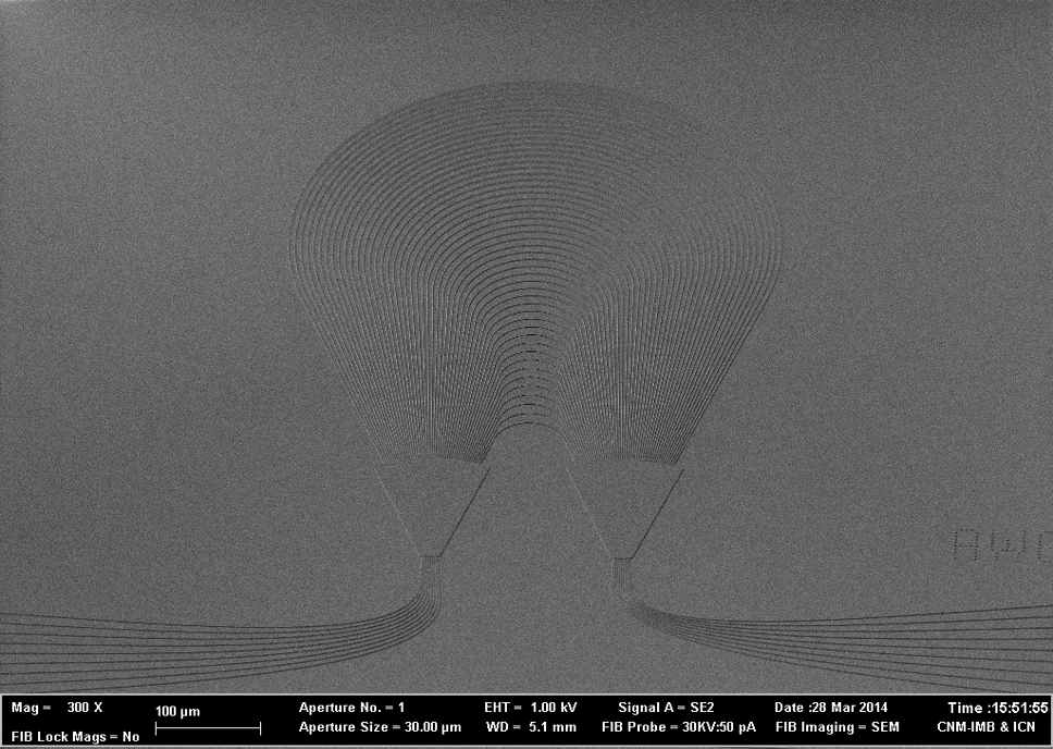
The Clean Room IMB-CNM includes equipment for CMOS and nanofabrication processes, using 100/150 mm wafers diameters. The total area is 1500 m2. Class 100-10,000 (ISO 5-7) depending on the areas. Aside from the process equipments, metrological techniques like ellipsometry, interferometry, AFM, SEM, FIB... are used for technological validation.
The process technical features are:
- Wavelength range from Visible to Mid infrared
- Three waveguide cross-sections (nitride film 300 nm height, shallow 150/300, deep 300 and mini-deep 150 nm)
- Thermo-optic tuners (10 nm Cr + 90 nm Au, Rsq= 0,3 Ω)
- Selective area trenching (evanescent sensors)
Technology
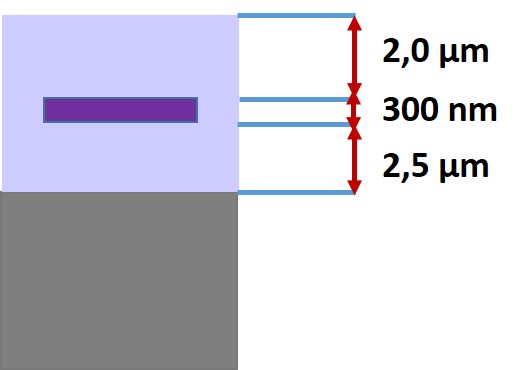
(1) Layerstack
- 4 inches silicon wafer 500 microns thick
- 2,5 microns thermal oxide substrate
- 300 nm Silicon Nitride film
- 2,0 microns top cladding
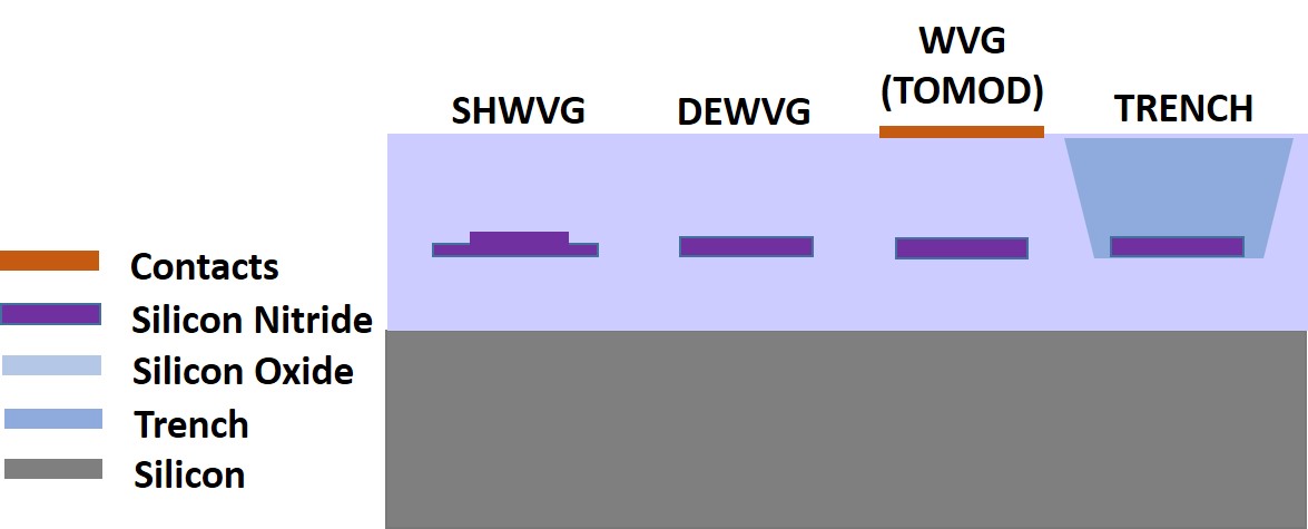
(2) Processing steps
- 1) Thermal oxide substrate → Oxidize 2,5 microns of the wafer (both sides)
- 2) LPCVD stoichometric silicon nitride deposition → 300 nm (both sides)
- 3) Shallow waveguide definition → lithography + 150 nm etching step
- 4) Deep waveguide definition → lithography + 300 nm etching step
- 5) Cladding deposition → 2,0 microns PECVD oxide
- 6) Selective area trench → lithography + 2,0 microns etching on top of the cladding
- 7) Metalization → lithography + Cr/Au stack patterned to include heaters
Design Manual / PDK
A design manual is available to the users of the platform:
Contains all the technology, related information and also all the required guidelines to simulate, design and submit contributions to the platform (i.e. refractive indices, GDS layers, logic and numbering, critical dimensions, simulation and measurement results).
- A Process Design Kit (PDK) is available, and it has also a design flow implemented for the Synopsys software.
- The PDK contains all the technology related information to ease and automate the design, simulation and layout of the user components.
- The PDK also contains the standard building blocks offered to the MPW users
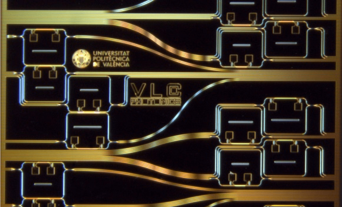
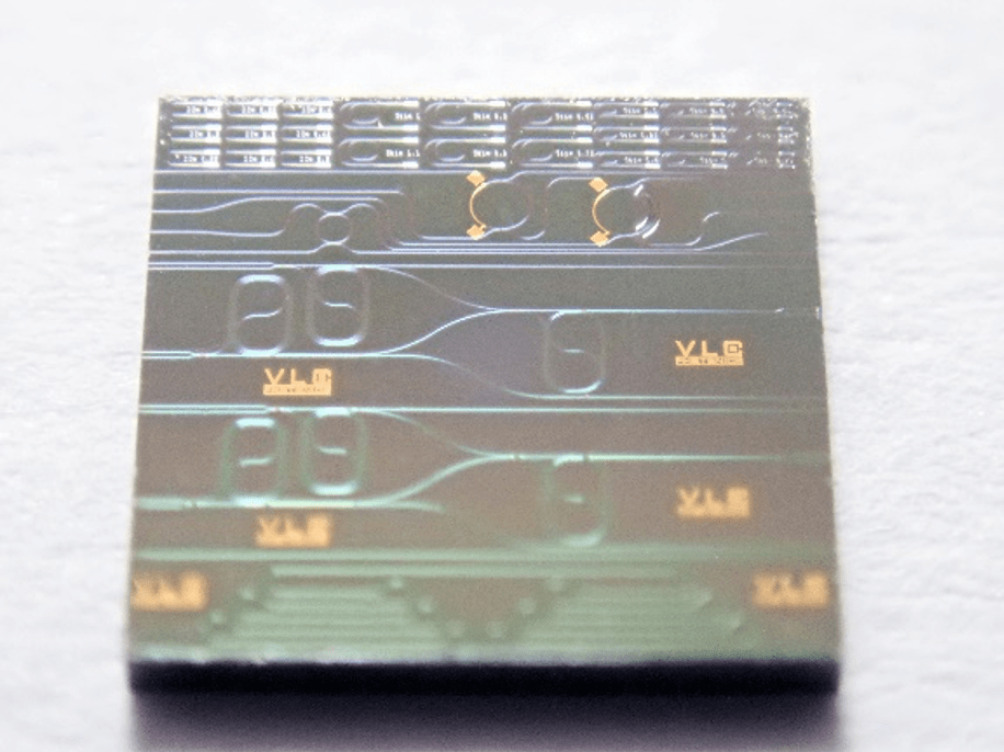
- Among others these building blocks are: spirals, symmetric and asymmetric 1x2 and 2x2 MMI splitters, shallow to deep and deep to shallow transitions, tapers/inverted tapers, ring and racetrack filters, reflectors, switches, vertical grating couplers, and tunable Interferometers.
- Information about the standard building blocks is also included in the manual.
MPW Model
- Fabrication process employs stepper lithography.
- Maximum reticle size 20 x 20 mm2.
- Reticle divided in smaller cells to share cost among users.
- Two cell sizes available:Fabrication process.
- medium: 5x5 mm (7 cells available + 1 PCM cell reserved for the CNM foundry)
- large: 5x10 mm (4 cells available)
- All the fabrication steps are common to all users (cost efficient).
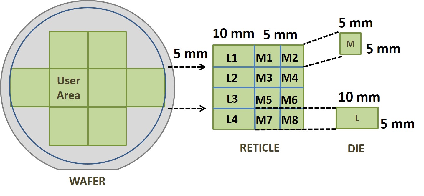
At least 20 die copies of each cell are delivered to the users. Pricing:
- Medium size: 7.500€
- Large size: 15.000€
(Custom PIC design and characterization trainings are also available by VLC Photonics. contact info@vlcphotonics.com for details.)
Custom Fabrication
Dedicated/custom Fabrication
CNM also offers the possibility of executing dedicated runs, using either the generic SiN process or any customization of it (different dielectric and metal materials, custom layer thicknesses, different or additional etch steps, etc.). Volumes can range between 1-25 wafers per batch, and fabrication in volume up to 300 wafers/month.
Moreover, a CNM proprietary process called Mix&Match allows the integration of nanometric patterns, by EBL, with standard lithography by Stepper.
Electrical wafer level testing service is also available at IMB-CNM, and optical wafer level testing is offered in collaboration with VLC Photonics.
Contact
For more information, please contact:
Carlos Dominguez
Tel.: +34 93 594 77 00
Carlos.Dominguez@imb-cnm.csic.es