The technology sanctuary where chips are forged to explore space or probe cells
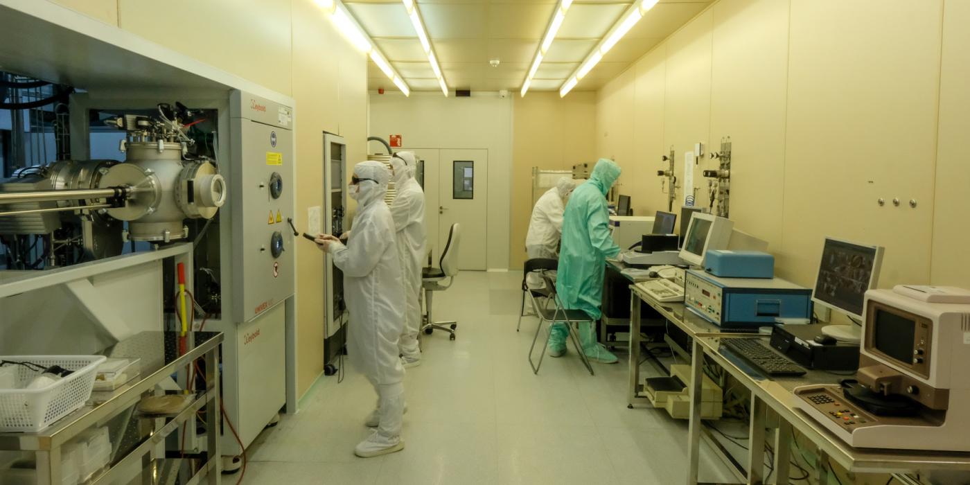
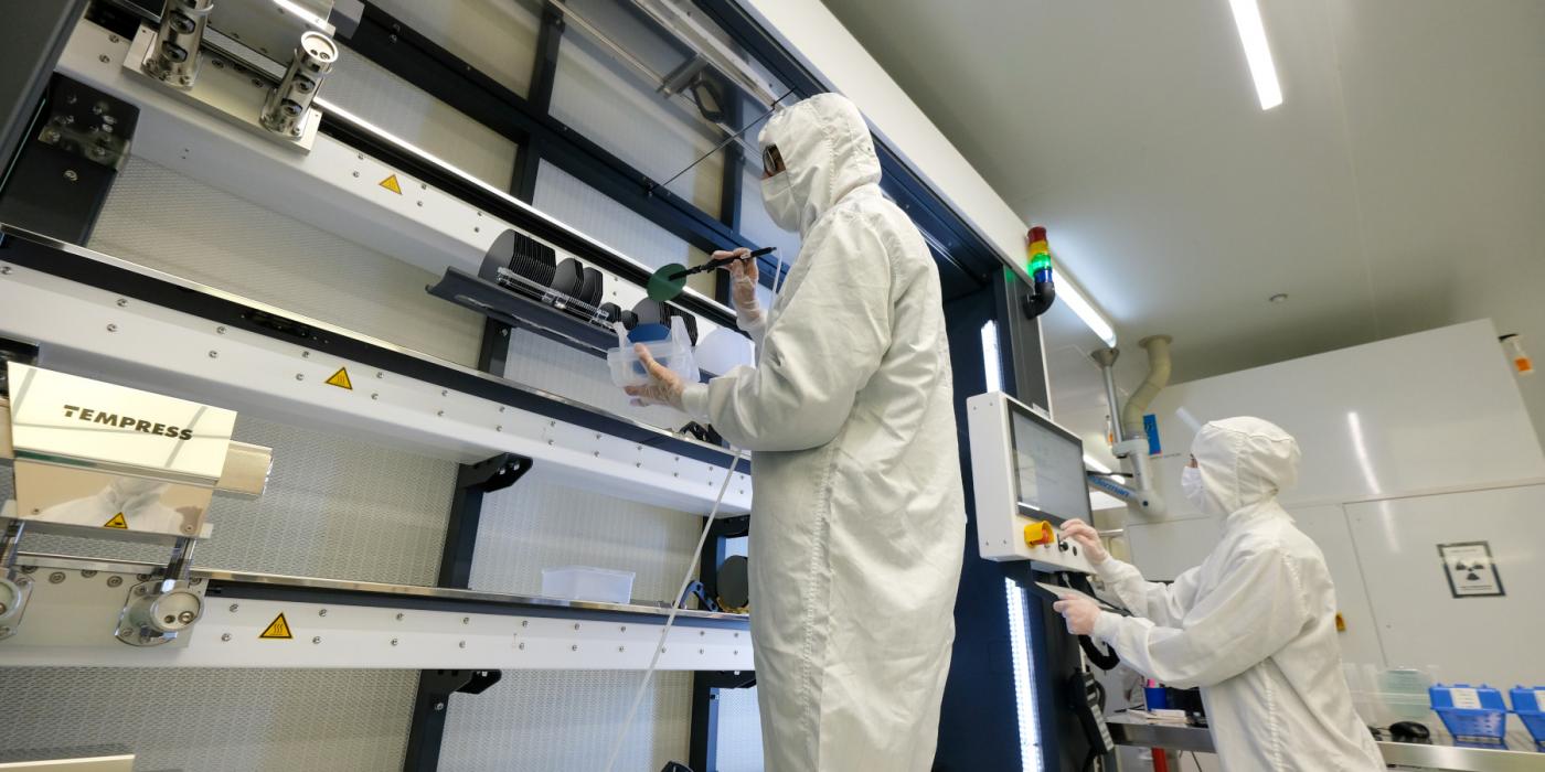
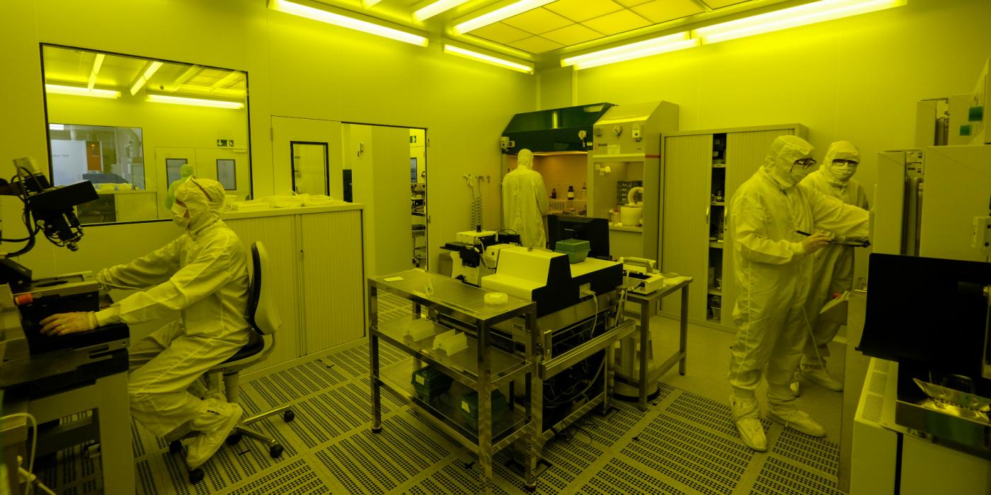
The IMB is home to an exceptional infrastructure: the largest clean room in southern Europe, a hyper-clean environment for manufacturing everything from integrated circuits to photonic and quantum chips.

The CSIC Investiga magazine has published a new issue dedicated to the challenges of the Digital Society, based on the CSIC's White Paper on Digital and Complex Information. The edition is coordinated by the same researchers who coordinated the white paper, Gemma Rius (from the Devices and Power Systems group) and Roberta Zambrini (from the Institute of Interdisciplinary Physics and Complex Systems of the CSIC, IFISC). Both are in charge of the editorial that opens the publication, which includes IMB-CNM research in data science, digital security, the manufacture of semiconductors and photonic and quantum devices. The following lines partially reproduce some paragraphs about IMB-CNM research that are included in the magazine.
The technology sanctuary where chips are forged to explore space or probe cells
The IMB is home to an exceptional infrastructure: the largest clean room in southern Europe, a hyper-clean environment for manufacturing everything from integrated circuits to photonic and quantum chips.
On the outskirts of Barcelona there is a kind of technological sanctuary, where objects of extreme purity are forged. Within its walls, the air must be extremely clean. Its workers carry out their tasks like monks dressed in special robes. The temperature, humidity and pressure - which is higher than outside - are kept constant to protect their precious jewels: microchips and nanodevices of utmost precision, which are going to travel into space, probe into neuronal connections of the brain and even into the innermost realms of our cells.
This technological sanctuary is the Micro and Nanofabrication Clean Room at IMB-CNM (Institute of Microelectronics of Barcelona), part of the CSIC. “These are exceptional facilities,” says its director, Luis Fonseca. “The clean room stands out in southern Europe in its category in terms of size (1,500 square metres), versatility (technologies in silicon, silicon carbide, etc.) and technological flexibility, being the best equipped, with nearly 200 pieces of equipment,” he adds.
In these facilities, located on the campus of the UAB (Universitat Autònoma de Barcelona) electronic devices and systems are designed and manufactured, which are able to manage information or to maintain physical-digital interaction with their environment. “We cover technologies ranging from the field of semiconductors and silicon micromachining to more novel ones, such as photonic circuits, quantum devices, silicon nanowires and one-atom-thick materials (two-dimensional materials),” says Fonseca.
Devices for space and for CERN
“In recent years we have achieved various milestones, such as fabricating nanochips to study living cells and components adapted to the hostile conditions of space missions, like those currently on their way to Mercury (BepiColombo) and the Sun (SolarOrbiter), created ad hoc, or those that orbit the Earth guiding satellites in the One Web constellation,” recounts the institute’s director.
IMB-CNM possesses the know-how to design and manufacture specific hardware capable of acquiring and processing huge volumes of data. “We have developed new radiation detectors for the accelerators of the Atlas experiment at CERN (with which the institute has been collaborating for over 20 years), enabling the acquisition of a host of particle detector channels,” says Fonseca.
Besides exploring space and delving into the bowels of matter, devices produced in the Clean Room are also being used to learn about the brain. “We have developed neural interfaces (within the European BrainCom project) based on graphene transistors that, by using multiplexing techniques, are able to increase the recording channels without increasing the number of connections,” explains the director. The integrated circuits designed at IMB-CNM have made it possible to process reams of information on brain activity.
Fonseca stresses that these technologies are consolidated. There is still a long way to go to meet current challenges, such as the new European RISC-V architecture processor designs that seek to alleviate European technological dependence (within the DRAC project). At the same time, the institute is also developing areas of research into new highly promising technologies.
Photonic technologies for telecommunications and energy
Photonics as an enabling technology is the great promise of the last decade, with potential applications as yet to be conceived. Light science and technology studies the generation, manipulation and detection of photons, particles that can be used as information carriers. Integrated photonics is present in many applications related to information processing, such as fibre optic telecommunications, laser printing, sensors, displays, smart lighting or photovoltaic systems.
“Just as microelectronics transformed the technological world of the 20th century, photonics is the technology best poised to continue advances in the digital world of the 21st century. Integrated photonic circuits will enable dramatic advances in quantum computing, quantum communications and quantum sensors,” explains Carlos Domínguez, IMB-CNM researcher and head of the SiN Photonics platform.
The IMB-CNM Clean Room houses a stable, open-access photonics platform, SiN Photonics, where a manufacturing process using silicon nitride technology has been developed in collaboration with the company VLC Photonics. Wafers for photonic applications can be fabricated and technologically validated in this special laboratory.
Potential in emerging technologies
The internet of things (IoT) works by interconnecting everyday data and devices via the internet or a network, where objects carry sensors that enable data exchange. It is used for process automation, home automation, sensor networks or mobile connections. The functional and energy autonomy of these devices is essential to enable their maximum deployment. Their development is key to the economy or the generation of renewable energy, which also implies a multiplication of mobile devices and small computers, which generate more consumption and electronic requirements.
Another key area is the development of electronic devices that operate with minimal power consumption, specifically through the application of advanced nanofabrication methods. IMB-CNM participated in the European ION4SET project, which focused on developing single-electron transistors (SET) based on silicon nanowires, allowing for greater integration and lower power dissipation. The objective was to manufacture a circuit integrating the SET with a traditional field effect transistor (FET) to work at room temperature with a much lower power consumption than a traditional circuit.
“We have been able to demonstrate the joint fabrication of SET and FET devices,” says Joan Bausells, who is responsible for IMB-CNM’s participation in the project. “Recent developments show that the integration of advanced low-power devices into electronic systems can facilitate the large-scale deployment of IoT devices,” he adds.
Research into nanomechanical and nanoelectronic devices to be integrated into miniaturised systems is aiming to provide solutions for future semiconductor-based quantum computers. Quantum devices require extreme precision in their fabrication.
Quantum devices
The IMB-CNM participates in establishing a pilot line for the manufacture of quantum devices compatible with the CMOS standard in the Clean Room, which will enable the creation of the first qubit or quantum-bit semiconductor in Spain. A qubit is the quantum analogue of the classical bit, with the particularity that it represents a combination of two states, giving rise to an exponential increase in computing capacity. This research centre also participates in a European consortium to develop fabrication lines for quantum technologies to be offered to academic and industrial users, Qu-Pilot.
“The goal is to have an affordable platform for quantum devices so research into technological solutions can improve device performance, as well as come up with new device concepts and their applications. It will be made available in open access through the Clean Room,” says Francesc Pérez-Murano. This research scientist, based at the IMB-CNM, is leading the centre’s contribution to qubit, its participation in the PTI+ QTEP (CSIC’s Quantum Technologies Platform) and in Qu-Pilot.
The institute also works on micro- and nano-processing capabilities by producing devices with advanced materials or superconducting functionalities. Quantum applications include scalable processors and ultra-sensitive sensors. “We are looking for developments based on the magnetism of nanostructured materials as a safe and energy-efficient alternative to conventional electronics-based information management,” explains Gemma Rius, a researcher at IMB-CNM.
All in all, the IMB Clean Room provides state-of-the-art infrastructure, driving the development of devices able to boost disruptive technologies, such as photonics and quantum computing, which will be key to the digital society of the future.
Hub of the clean-room network
The Clean Room is recognised as a Unique Scientific and Technical Infrastructure (ICTS) by the Spanish Ministry for Science and Innovation (MCIN). It is the hub of Micronanofabs, a national clean-room network, and openly offers its services to research groups andcompanies (including MPS, Fagor Electrónica, Devicare, SolarMems, Qilimanjaro, Inbrain Neuroelectronics). It forms part of Euronanolab, the European network of clean-room facilities, and articipates in NFFA-Pilot, the European access programme in nanotechnology.
Exfiles: big data against crime
The European project Exfiles is developing different hardware and software methods to extract data from smartphones used by criminals that can serve as forensic evidence in a judicial process. In a state-of-the-art mobile phone, accessing encrypted information requires "disassembling the integrated circuit layer by layer until locating the 'place' where that information is found," explains Salvador Hidalgo. It is a process that requires the analysis of massive amounts of data.
"Sometimes an invented encryption key is entered into the phone, and when it verifies that it is not correct, it returns an error message. This action is repeated thousands of times to observe the energy consumption of the chip in these operations. Later, by analyzing this data, it is possible to discover what the secret key is. But we need a computer that repeats this cycle over and over again for hours", says Jofre Pallarès about the work process.
Pallarès and Hidalgo are IMB-CNM researchers on the project, which brings together a consortium of research centers, universities, cybersecurity companies and forensic groups from five police agencies.