


Home
News
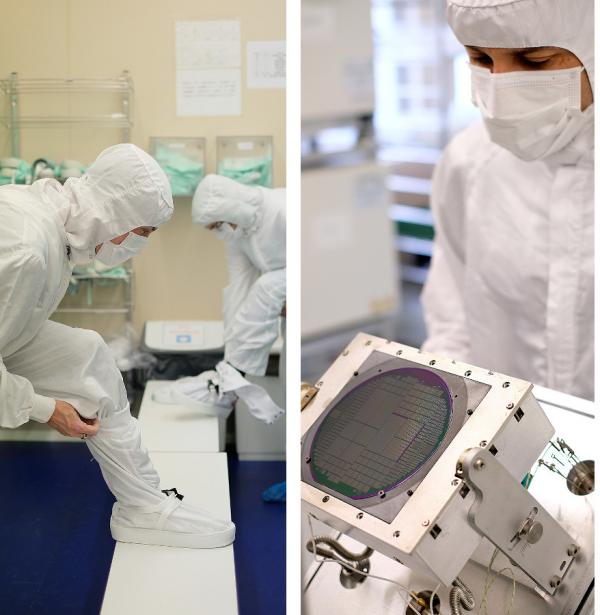
The Institute of Microelectronics of Barcelona receives the María de Maeztu distinction of excellence
The IMB-CNM, a CSIC institute dedicated to micro and nanoelectronics, joins the network of centers accredited as a María de Maeztu Unit of Excellence, awarded by the State Research Agency, for the next six years.
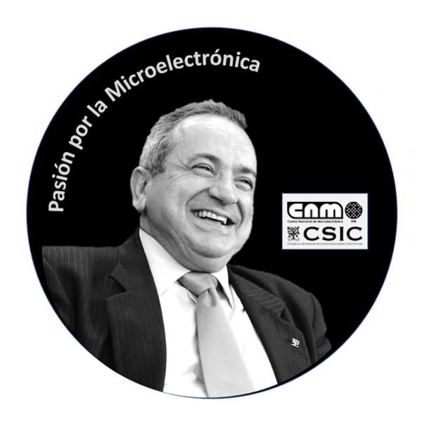
Emilio Lora-Tamayo (1950-2024). Pasión por la Microelectrónica
La trayectoria de Emilio Lora-Tamayo d’Ocón, exdirector y vicedirector del IMB-CNM: una visión personal de sus compañeros.
Agenda
Highlights
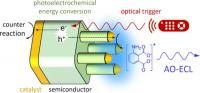
Electrochemiluminescence (ECL) is widely employed for medical diagnosis and imaging. Despite its remarkable analytical performances, the technique remains intrinsically limited by the essential need for an external power supply and electrical wires for electrode connections. Here, we report an electrically autonomous solution leading to a paradigm change by designing a fully integrated all-optical wireless monolithic photoelectrochemical device based on a nanostructured Si photovoltaic junction modified with catalytic coatings. Under illumination with light ranging from visible to near-infrared, photogenerated holes induce the oxidation of the ECL reagents and thus the emission of visible ECL photons. The blue ECL emission is easily viewed with naked eyes and recorded with a smartphone. A new light emission scheme is thus introduced where the ECL emission energy (2.82 eV) is higher than the excitation energy (1.18 eV) via an intermediate electrochemical process. In addition, the mapping of the photoelectrochemical activity by optical microscopy reveals the minority carrier interfacial transfer mechanism at the nanoscale. This breakthrough provides an all-optical strategy for generalizing ECL without the need for electrochemical setups, electrodes, wiring constraints, and specific electrochemical knowledge. This simplest ECL configuration reported so far opens new opportunities to develop imaging and wireless bioanalytical systems such as portable point-of-care sensing devices.
Journal of the American Chemical Society 2023 145 (31), 17420-17426. DOI: 10.1021/jacs.3c05856
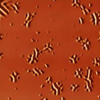
The understanding of the dynamics of a glass above its devitrification temperature remains incomplete. Here, we build a spatio-temporal map of the relaxation dynamics of a highly stable glass into its supercooled liquid using real-time atomic force microscopy imaging. This methodology enables direct visualization of the progression of the liquid phase and clarifies and quantifies the presence of localized fast mobility regions separated by giant length scales. Our data establish a clear correlation between dynamic length and time scales in glasses. This approach may also be applicable to unveil the microscopic structure and dynamics of other glass-forming systems with much shorter length and time scales, including liquid-cooled glasses.